
LED packaging method improving color zone in-BIN rate

A LED packaging and color zone technology, applied in electrical components, circuits, semiconductor devices, etc., can solve problems such as uneven precipitation, non-concentrated color zone targeting, and changes in electrical parameters of LED products, so as to improve shipment rate and material The effect of increasing the rate of entry into BIN

Inactive Publication Date: 2016-08-10
CHANGZHI HONGYUAN PHOTOELECTRIC TECH
View PDF0 Cites 0 Cited by
  • Summary
  • Abstract
  • Description
  • Claims
  • Application Information

AI Technical Summary

Problems solved by technology

[0002] In the field of LED packaging, the packaging process is to use packaging glue to encapsulate the surface of the material that has been solidified and wire-bonded to complete the packaging process. However, in order to reduce the production cost of current LED products, in order to reduce the production cost, the chip is selected Most of the time, wafers with a relatively wide band and no chip screening are used. In this way, when splitting light, the color area of ​​the material is not concentrated due to the wide span of the chip band, and the rate of entering the BIN of the color area is low; when using encapsulant After the packaging is completed, the LED product is baked in a short period of time (generally about 10 minutes). The low rate of entering the BIN in the color area during light splitting results in a low shipment rate of LED white light products

Method used


Image

  • LED packaging method improving color zone in-BIN rate

Examples


Embodiment Construction

[0012] In order to make the purpose, technical solutions and advantages of the embodiments of the present invention clearer, the technical solutions in the embodiments of the present invention will be clearly and completely described below in conjunction with the drawings in the embodiments of the present invention. Obviously, the described embodiments It is a part of the embodiments of the present invention, rather than all embodiments; based on the embodiments of the present invention, all other embodiments obtained by those of ordinary skill in the art without creative work, all belong to the protection scope of the present invention .

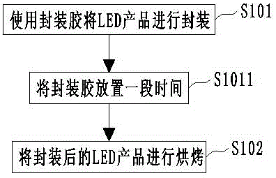
[0013] figure 1 A schematic flow chart of an LED packaging method with a higher color zone entering BIN rate provided in Embodiment 1 of the present invention, as shown in figure 1 As shown, a LED packaging method with a higher color zone entering BIN rate includes steps:

[0014] S101: Encapsulate the LED product with encapsulation glue....


PUM


Abstract

The invention belongs to the technical field of LEDs, and specifically relates to an LED packaging method with a higher color zone entering BIN rate; the technical problem to be solved is: to provide a high color zone entering BIN rate that improves the shipment rate of LED white light products LED encapsulation method; the adopted technical scheme is: an LED encapsulation method with a higher color area into BIN rate, including the steps: S101: encapsulating the LED product with encapsulation glue; S102: baking the encapsulated LED product Baking; after the step S101, further include: S1011: leave the encapsulation glue for a period of time; the present invention is applicable to the LED field.

Description

technical field [0001] The invention belongs to the technical field of LEDs, and in particular relates to an LED packaging method with a relatively high BIN ratio in color regions. Background technique [0002] In the field of LED packaging, the packaging process is to use packaging glue to encapsulate the surface of the material that has been solidified and wire-bonded to complete the packaging process. However, in order to reduce the production cost of current LED products, in order to reduce the production cost, the chip is selected Most of the time, wafers with a relatively wide band and no chip screening are used. In this way, when splitting light, the color area of ​​the material is not concentrated due to the wide span of the chip band, and the rate of entering the BIN of the color area is low; when using encapsulant After the packaging is completed, the LED product is baked in a short period of time (generally about 10 minutes). This caused the low rate of entering ...

Claims


Application Information

Patent Timeline
Patent Type & Authority Applications(China)
IPC IPC(8): H01L33/50H01L33/52
CPCH01L33/50H01L33/52H01L2933/0041H01L2933/005
Inventor 靳亚男
Owner CHANGZHI HONGYUAN PHOTOELECTRIC TECH
Learn More