Array substrate, liquid crystal display panel, and liquid crystal display device

An array substrate and base material technology, applied in the field of liquid crystal display, can solve the problems of affecting the display effect, flickering, reducing the pixel aperture ratio, etc., to achieve the effect of ensuring the display effect, increasing the storage capacitance, and reducing the pixel aperture ratio

Active Publication Date: 2016-09-28
WUHAN CHINA STAR OPTOELECTRONICS TECH CO LTD
View PDF10 Cites 21 Cited by
  • Summary
  • Abstract
  • Description
  • Claims
  • Application Information

AI Technical Summary

Problems solved by technology

[0002] TFT (Thin Film Transistor, Thin Film Transistor) will generate leakage when grayscale voltage is applied, which will cause LCD (Liquid Crystal Display, Liquid Crystal Display) to produce flicker (Flicker) phenomenon and affect the display effect
In order to prevent the grayscale change of the pixel electrode caused by electric leakage and improve or avoid the flicker phenomenon, the LCD needs to have a larger storage capacitor, but a larger storage capacitor requires two larger plates, namely the common electrode of the array substrate and the size of the pixel electrode is larger, which will undoubtedly reduce the aperture ratio of the pixel

Method used


Image

  • Array substrate, liquid crystal display panel, and liquid crystal display device
  • Array substrate, liquid crystal display panel, and liquid crystal display device
  • Array substrate, liquid crystal display panel, and liquid crystal display device

Examples


Embodiment Construction

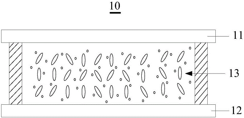
[0026] figure 1 is a cross-sectional view of the structure of a liquid crystal display panel according to an embodiment of the present invention. like figure 1 As shown, the liquid crystal display panel 10 of this embodiment includes a color filter substrate (Color Filter Substrate, referred to as CF substrate, also known as color filter substrate) 11 and an array substrate (Thin Film Transistor Substrate, referred to as TFT substrate, also known as Thin film transistor substrate (or Array substrate) 12 and liquid crystal (liquid crystal molecules) 13 filled between the two substrates, the liquid crystal 13 is located in the liquid crystal cell formed by stacking the array substrate 12 and the color filter substrate 11 .

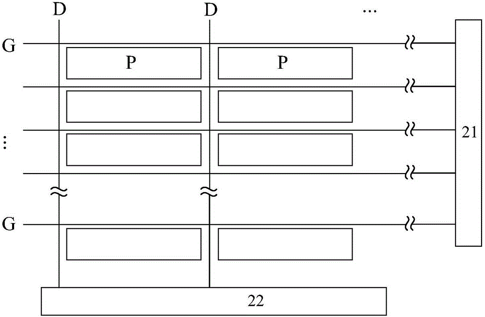
[0027] combine figure 2 A schematic diagram of the pixel structure of the liquid crystal display panel 10 shown, the array substrate 12 includes a plurality of data lines D arranged along the column direction, a plurality of scan lines G arranged along th...


PUM


Abstract

The invention discloses an array substrate, a liquid crystal display panel, and a liquid crystal display device. A metal layer is arranged between a pixel electrode and a common electrode; and the metal layer and the pixel electrode form a first storage capacitor and the common electrode forms a second storage capacitor, thereby forming a dual-storage capacitor unit. Therefore, the storage capacitance is increased; a scintillation phenomenon caused by TFT electricity leakage is avoided; and a display effect is guaranteed. Moreover, the two storage capacitors are superposed, so that no pixel aperture opening rate is reduced.

Description

technical field [0001] The present invention relates to the technical field of liquid crystal display, in particular to an array substrate, a liquid crystal display panel and a liquid crystal display device. Background technique [0002] TFT (Thin Film Transistor, Thin Film Transistor) will generate leakage current when grayscale voltage is applied, which will cause LCD (Liquid Crystal Display, Liquid Crystal Display) to produce flicker (Flicker) phenomenon, and affect the display effect. In order to prevent the grayscale change of the pixel electrode caused by electric leakage and improve or avoid the flicker phenomenon, the LCD needs to have a larger storage capacitor, but a larger storage capacitor requires two larger plates, that is, the common electrode of the array substrate And the size of the pixel electrode is larger, which will undoubtedly reduce the aperture ratio of the pixel. Contents of the invention [0003] In view of this, the embodiments of the present i...

Claims


Application Information

Patent Timeline
Patent Type & Authority Applications(China)
IPC IPC(8): H01L27/12G02F1/1362
CPCG02F1/136213G02F1/136227H01L27/124H01L27/1255G02F1/13338G02F1/134318G02F1/133345G02F1/1368G02F2201/121G02F2201/123G02F1/133357
Inventor 马亮
Owner WUHAN CHINA STAR OPTOELECTRONICS TECH CO LTD
Why Eureka
Try Eureka