Three-dimensional semiconductor memory device and method of fabricating the same

A technology of storage devices and semiconductors, which is applied in semiconductor/solid-state device manufacturing, semiconductor devices, semiconductor/solid-state device components, etc., and can solve problems such as the limitation of integration density of 2D storage devices

Inactive Publication Date: 2016-10-12
SAMSUNG ELECTRONICS CO LTD
View PDF2 Cites 28 Cited by
  • Summary
  • Abstract
  • Description
  • Claims
  • Application Information

AI Technical Summary

Problems solved by technology

However, the integration density of 2D memory devices continues to increase but remains limited due to the need for extremely expensive devices to form fine patterns

Method used


Image

  • Three-dimensional semiconductor memory device and method of fabricating the same
  • Three-dimensional semiconductor memory device and method of fabricating the same
  • Three-dimensional semiconductor memory device and method of fabricating the same

Examples


Embodiment Construction

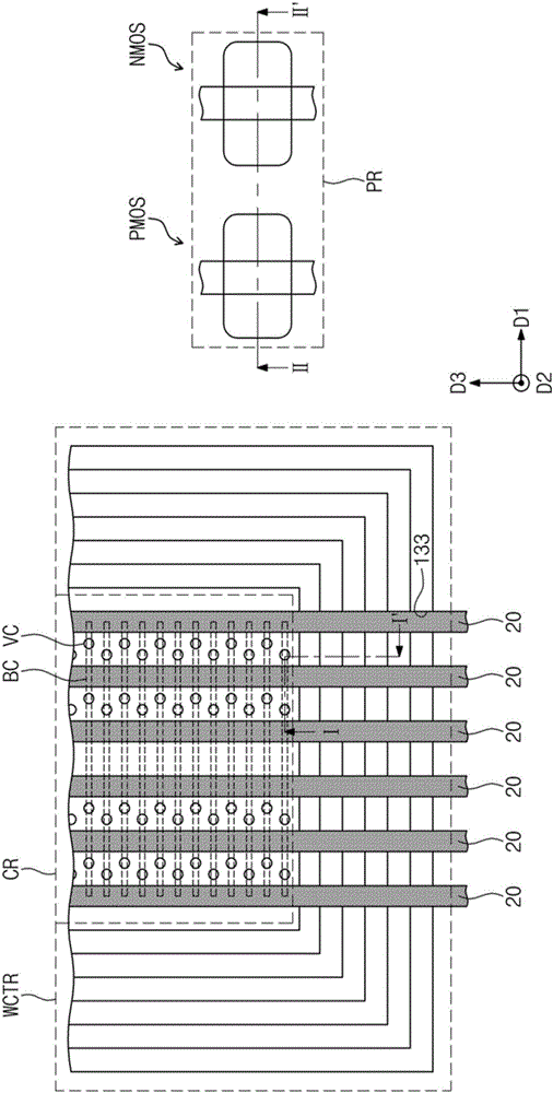
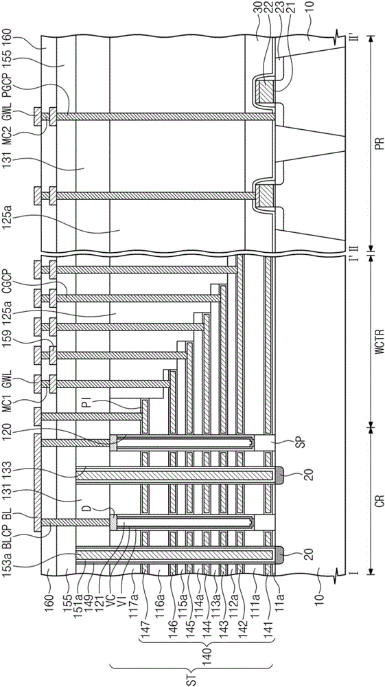
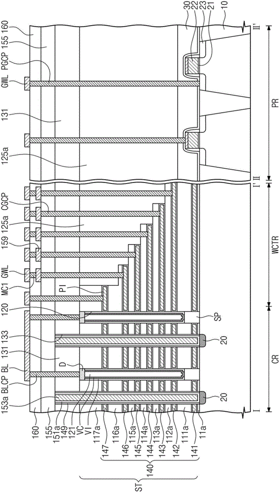
[0026] The inventive concept will now be described more fully hereinafter with reference to the accompanying drawings, in which exemplary embodiments of the inventive concept are shown. The advantages and features of the inventive concept and methods of achieving them will be apparent through the following exemplary embodiments, which will be described in more detail with reference to the accompanying drawings. It should be noted, however, that the inventive concept is not limited to the following exemplary embodiments, and can be implemented in various forms. Therefore, the exemplary embodiments are merely provided for disclosing the inventive concept and making the category of the inventive concept known to those skilled in the art. In the drawings, embodiments of the inventive concept are not limited to the specific examples provided herein and are exaggerated for clarity.

[0027] The terminology used herein is for the purpose of describing particular embodiments only and...


PUM


Abstract

A semiconductor memory device is provided including a substrate; a stack structure including gate electrodes vertically stacked on the substrate; a vertical channel part penetrating the gate electrodes; a dopant region provided in the substrate at a side of the stack structure; a common source plug on the substrate and electrically connected to the dopant region; and cell contact plugs connected to the gate electrodes, respectively. A top surface of the common source plug is at a different level from top surfaces of the cell contact plugs.

Description

technical field [0001] The inventive concepts relate generally to semiconductor devices, and more particularly, to semiconductor memory devices and methods of manufacturing the same. Background technique [0002] Semiconductor devices have been highly integrated to provide high performance and reduce cost. Specifically, the integration density of a semiconductor memory device will directly affect the cost of the semiconductor memory device. The integration density of a conventional two-dimensional (2D) memory device may be mainly determined by the area occupied by a unit memory cell, and thus may be greatly affected by a technique for forming a fine pattern. However, since extremely expensive devices are required to form fine patterns, the integration density of 2D memory devices continues to increase but is still limited. [0003] To overcome these limitations, 3D semiconductor memory devices including three-dimensionally arranged memory cells have been developed. Conte...

Claims


Application Information

Patent Timeline
Patent Type & Authority Applications(China)
IPC IPC(8): H01L27/115H01L21/8247
CPCH10B43/20H10B43/27H10B43/10H10B43/50H10B43/40H01L23/528H01L23/5226
Inventor 姜周宪车俊昊玄忠一
Owner SAMSUNG ELECTRONICS CO LTD
Why Eureka
Try Eureka