display device

A display device and pixel technology, applied in static indicators, instruments, nonlinear optics, etc., can solve problems such as display quality degradation

Active Publication Date: 2019-09-20
JAPAN DISPLAY INC
View PDF4 Cites 0 Cited by
  • Summary
  • Abstract
  • Description
  • Claims
  • Application Information

AI Technical Summary

Problems solved by technology

Therefore, it is necessary to prevent the degradation of display quality due to metal wiring

Method used


Image

  • display device
  • display device
  • display device

Examples


no. 1 approach

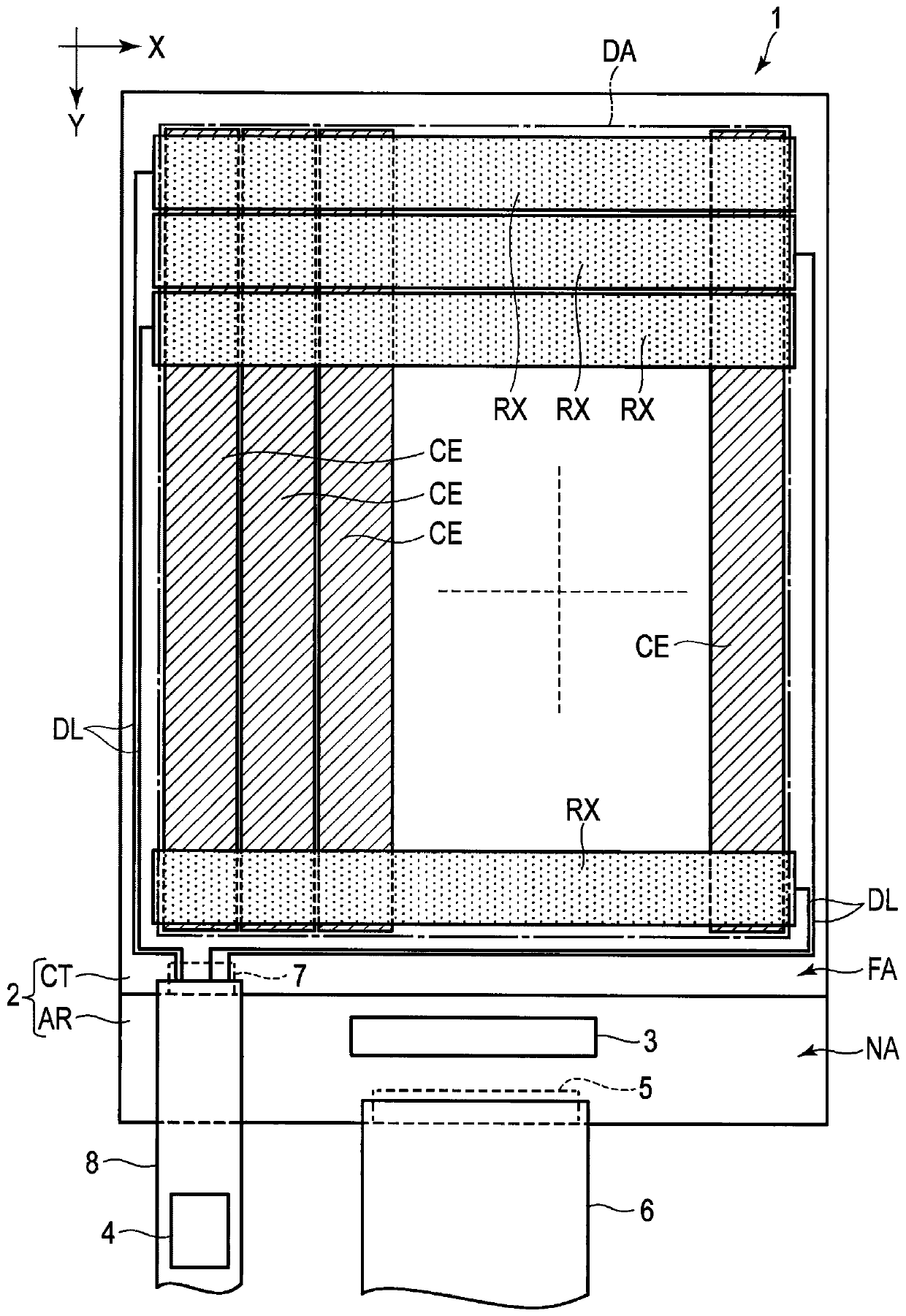
[0029] figure 1 It is a plan view showing a schematic configuration of the liquid crystal display device 1 of the first embodiment. The liquid crystal display device 1 can be used in various devices such as smartphones, tablet terminals, mobile terminals, personal computers, television receivers, vehicle-mounted devices, game devices, and wearable terminals.

[0030] The liquid crystal display device 1 has a display panel 2 , a plurality of common electrodes CE, a plurality of detection electrodes RX facing each common electrode CE, a driver IC 3 functioning as a driver block, and a touch detection IC 4 functioning as a detection block.

[0031] The display panel 2 includes a rectangular array substrate AR (first substrate) and a rectangular counter substrate CT (second substrate) whose outer shape is smaller than that of the array substrate AR. exist figure 1 In the example of , the array substrate AR and the counter substrate CT are laminated so that three sides overlap ea...

no. 2 approach

[0094] The second embodiment will be described. The same reference numerals are assigned to the same or similar elements as those of the first embodiment. In addition, the structure which is not mentioned especially is the same as 1st Embodiment.

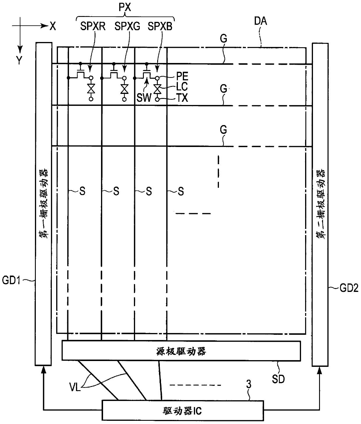
[0095] Figure 10 It is a plan view schematically showing an example of the layout of the metal wiring ML and the common electrode CE (configuration electrode SE) in the second embodiment. In the example shown in the figure, the metal wiring MLa is not formed in a region overlapping the scanning signal line G. As shown in FIG. That is, the metal wiring MLa is intermittently formed in the second direction Y. As shown in FIG.

[0096] In the present embodiment, the above-described first and second aspects are also applied to the metal lines MLa arranged along the second direction Y (or the direction in which the video signal lines S extend). That is, in a certain slit SL, the metal wiring MLa overlaps the constituent electrode SE ...

no. 3 approach

[0110] The third embodiment will be described. The same reference numerals are assigned to the same or similar elements as those of the first embodiment. In addition, the structure which is not mentioned especially is the same as 1st Embodiment.

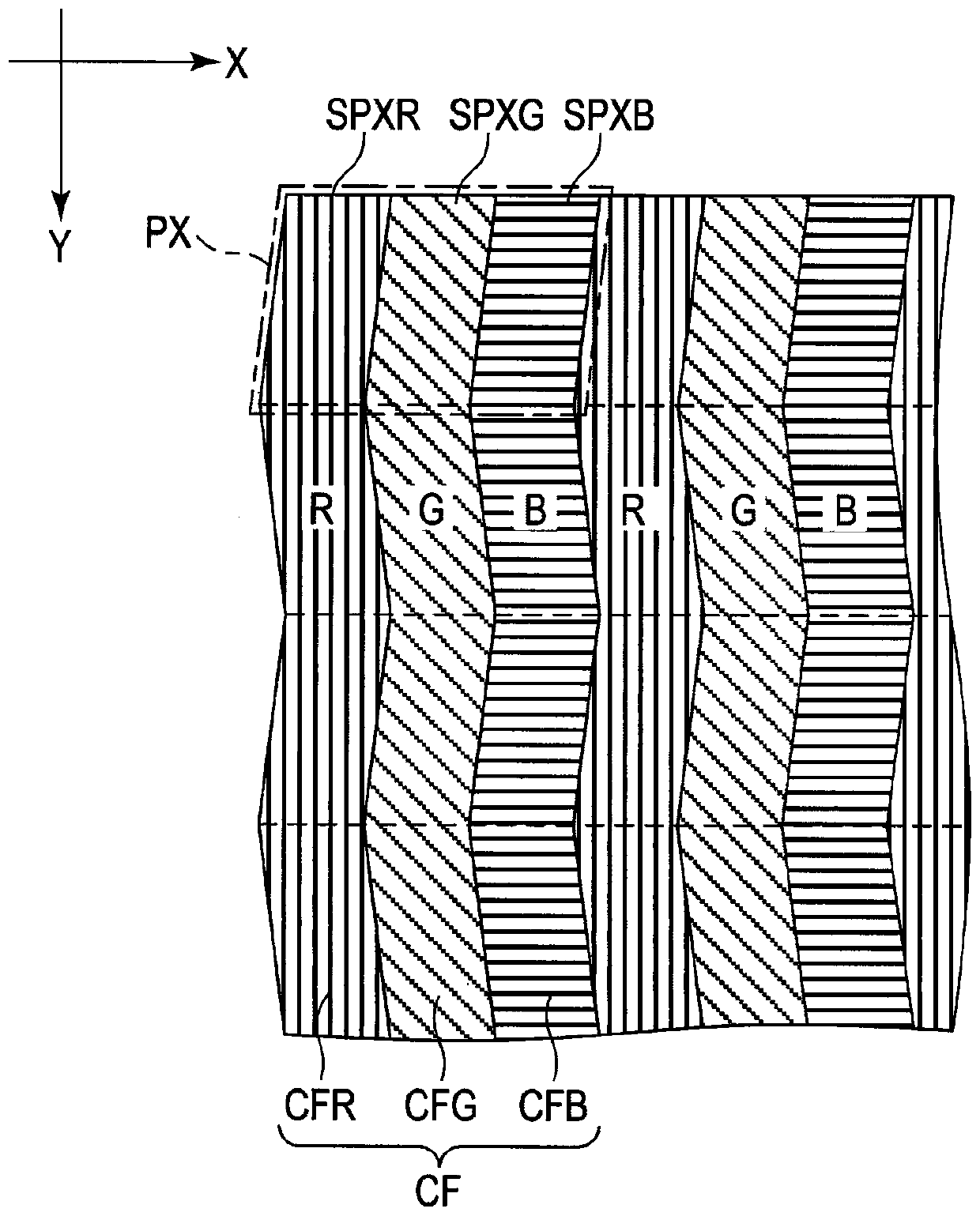
[0111] Figure 11 It is a plan view schematically showing the structure of the metal wiring ML in the third embodiment. In this embodiment, the metal wiring MLa extends continuously along the video signal line S basically the same as in the first embodiment. However, the metal wiring MLa is disconnected in the vicinity of the spacer SP so as not to overlap with the spacer SP in plan view.

[0112] A plurality of spacers SP are arranged between the array substrate AR and the counter substrate CT, and a cell gap is formed between the first alignment film 14 and the second alignment film 22 . The spacer SP may extend from the array substrate AR, and may also extend from the opposite substrate CT. The formation position of the space...


PUM


Abstract

A display device according to an embodiment of the present invention has a plurality of metal wirings in contact with constituent electrodes. The first filter overlaps the first and third pixels, and the second filter overlaps the second and fourth pixels. The first to fourth constituent electrodes overlap with the first to fourth pixels, respectively. The first slit extends between the first pixel and the second pixel in the extending direction of the first image signal line, and the second slit extends between the third pixel and the fourth pixel in the extending direction of the second image signal line extend. The first metal wiring is formed between the first and second constituent electrodes and covers a part of the first slit, and the second metal wiring is formed between the third and fourth constituent electrodes and covers a part of the second slit. The distance between the first metal wiring and the first constituting electrode is shorter than the distance between the first metal wiring and the second constituting electrode, and the distance between the second metal wiring and the fourth constituting electrode is shorter than the distance between the second metal wiring and the second constituting electrode. The distance between the three constituent electrodes is shorter.

Description

[0001] This application is based on the priority of Japanese Patent Application No. 2015-201909 filed on October 13, 2015, and the entire contents of this Japanese Patent Application are incorporated into this application by reference. technical field [0002] Embodiments of the present invention relate to a display device. Background technique [0003] Conventionally, there is known a liquid crystal display device including a pair of substrates and a liquid crystal layer sealed between the substrates. The liquid crystal display device displays an image by driving liquid crystal molecules of the liquid crystal layer using an electric field generated between a pixel electrode provided for each pixel and a common electrode passing through a plurality of pixels. [0004] The common electrode is composed of electrodes corresponding to the respective pixels (hereinafter referred to as constituent electrodes), and these constituent electrodes may be separated by slits. For exampl...

Claims


Application Information

Patent Timeline
Patent Type & Authority Patents(China)
IPC IPC(8): G02F1/133G02F1/1333G02F1/1362
CPCG02F1/133G02F1/13338G02F1/136286G02F1/134363G02F1/133514G02F1/134318G02F1/136218G02F1/134309G02F1/133308G02F1/13394G02F2201/121
Inventor 关健太小出元前出优次广泽仁
Owner JAPAN DISPLAY INC
Why Eureka
Try Eureka