VLSI (Very Large Scale Integration) layout design method for solving given border constraint

A technology of layout design and border, applied in CAD circuit design, calculation, special data processing applications, etc., can solve problems such as difficult to solve directly, large scale, etc., to meet the needs of layout planning and design, and effectively and practically the effect of layout planning results

Inactive Publication Date: 2017-05-31
FUZHOU UNIV
View PDF4 Cites 4 Cited by
  • Summary
  • Abstract
  • Description
  • Claims
  • Application Information

AI Technical Summary

Problems solved by technology

Due to the large scale of the VLSI layout problem, it is difficult for existing structure-based floorplanning design tools to solve it directly

Method used


Image

  • VLSI (Very Large Scale Integration) layout design method for solving given border constraint
  • VLSI (Very Large Scale Integration) layout design method for solving given border constraint
  • VLSI (Very Large Scale Integration) layout design method for solving given border constraint

Examples


Embodiment Construction

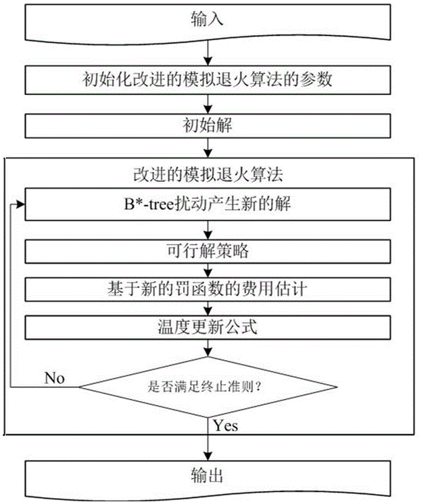
[0062] The technical solution of the present invention will be specifically described below in conjunction with the accompanying drawings.

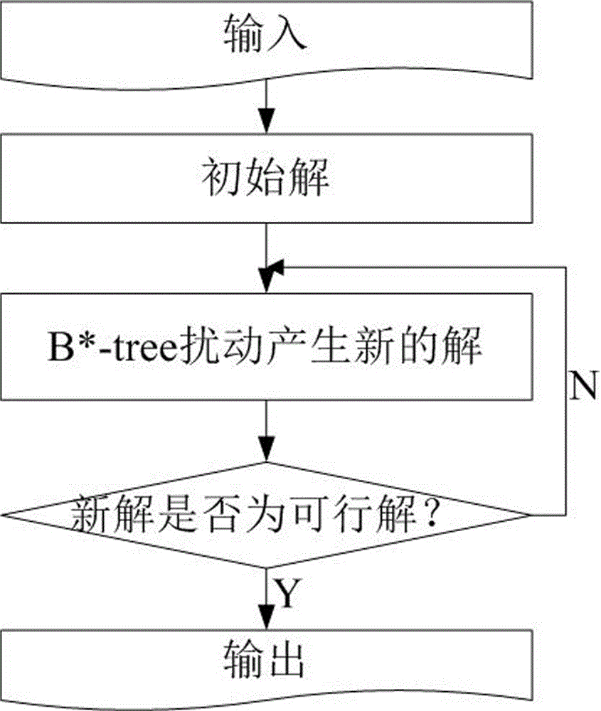
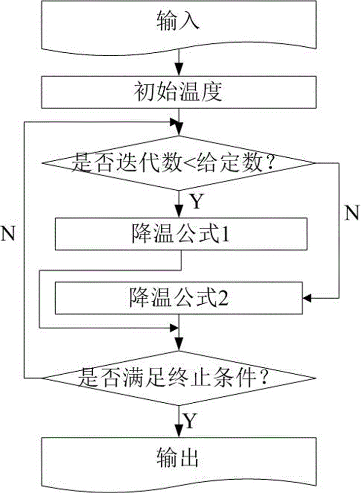
[0063] The invention provides a VLSI layout design method for solving a given border constraint, and aims to use a hybrid simulated annealing algorithm to deal with the layout planning problem of a given border constraint that cannot be divided into two in VLSI. The algorithm uses a penalty function based on the combination of the area violation function and the length violation function, and then uses the feasible solution strategy to make the new solutions that satisfy the bounding box constraints feasible solutions. Finally, the hybrid simulated annealing algorithm is used to search the solution space of the problem. Therefore, a layout planning result with a given border constraint based on an iterative method with superior performance is obtained.

[0064] Furthermore, the present invention proposes a hybrid simulated annealing-based...


PUM


Abstract

The invention relates to a VLSI (Very Large Scale Integration) layout design method for solving a given border constraint. By adopting a strategy of randomization, a random initial layout is used as an initial solution of a hybrid simulated annealing algorithm. The border constraint is proposed as a violating penalty function of a target function. The violating penalty function introduces a length function considering each module over a given border based on an area function considering a minimum rectangle enclosing candidate layout results over the given border. Based on the hybrid simulated annealing algorithm, a feasible solution strategy is introduced. Solutions produced via a series B*-tree disturbance are feasible solutions, so that better solutions can be obtained from the algorithm. The optimal solution is searched by introducing the hybrid simulated annealing algorithm, and a new temperature update formula is adopted in the algorithm. The new temperature update formula shortens the time for solving the spatial search phase, and more time is used for searching the better solutions in the temperature rise phase, so that the probability of finding the optimal solution is improved.

Description

technical field [0001] The invention relates to the technical field of VLSI physical design automation, in particular to a VLSI layout design method for solving given frame constraints. Background technique [0002] In recent years, with the rapid development of integrated circuit manufacturing technology, the integrated circuit industry has entered the era of nanotechnology, the integration of chips has been further improved, and more and more circuit components can be integrated on a chip. The VLSI design method has been proposed higher requirement. Layout planning is a very important link in the VLSI physical design process, which has a significant impact on the performance indicators of integrated circuits, such as routability, delay characteristics, power consumption, and circuit reliability. With the increasing constraints of the floorplanning problem and the rapid growth of the number of cells on the chip, the algorithm design of the VLSI floorplanning problem poses ...

Claims


Application Information

Patent Timeline
Patent Type & Authority Applications(China)
IPC IPC(8): G06F17/50
CPCG06F30/39
Inventor 陈建利刘岩朱自然朱文兴
Owner FUZHOU UNIV
Why Eureka
Try Eureka