Shift register, driving method thereof, gate driving circuit and display device

A technology of shift registers and potentials, which is applied in static memory, digital memory information, instruments, etc., can solve the problems of inability to realize low-frequency, low-power drive, etc., and achieve the effect of low-power drive

Active Publication Date: 2020-01-31
BOE TECH GRP CO LTD +1
View PDF5 Cites 0 Cited by
  • Summary
  • Abstract
  • Description
  • Claims
  • Application Information

AI Technical Summary

Problems solved by technology

However, the driving frequency (the ratio of the duration of the high level to the low level of the gate drive signal) of the shift registers at each level in the existing GOA circuit is fixed, which is only affected by the INPUT inputted by the shift register of the current level. signal (the gate drive signal output by the upper stage shift register), so it is impossible to achieve low frequency and low power consumption drive

Method used


Image

  • Shift register, driving method thereof, gate driving circuit and display device
  • Shift register, driving method thereof, gate driving circuit and display device
  • Shift register, driving method thereof, gate driving circuit and display device

Examples


Embodiment 1

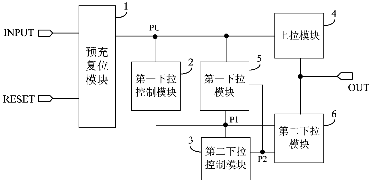
[0053] figure 1 A schematic structural diagram of a shift register provided in Embodiment 1 of the present invention, as shown in figure 1 As shown, the shift register includes: a pre-charge reset module 1, a first pull-down control module 2, a second pull-down control module 3, a first pull-down module 5, a second pull-down module 6 and a pull-up module 4, wherein, The pre-charge reset module 1, the first pull-down control module 2, and the pull-up module 4 are connected to the pull-up node PU, and the first pull-down control module 2, the first pull-down module 5, and the second pull-down module 6 are connected to the first pull-down node PU. The pull-down node P1, the second pull-down module 6, the first pull-down module 5, and the second pull-down module 6 are connected to the second pull-down node P2, and the second pull-down control module 3 is also connected to the first pull-down node P1.

[0054] The precharge reset module 1 is used to precharge or reset the pull-up ...

Embodiment 2

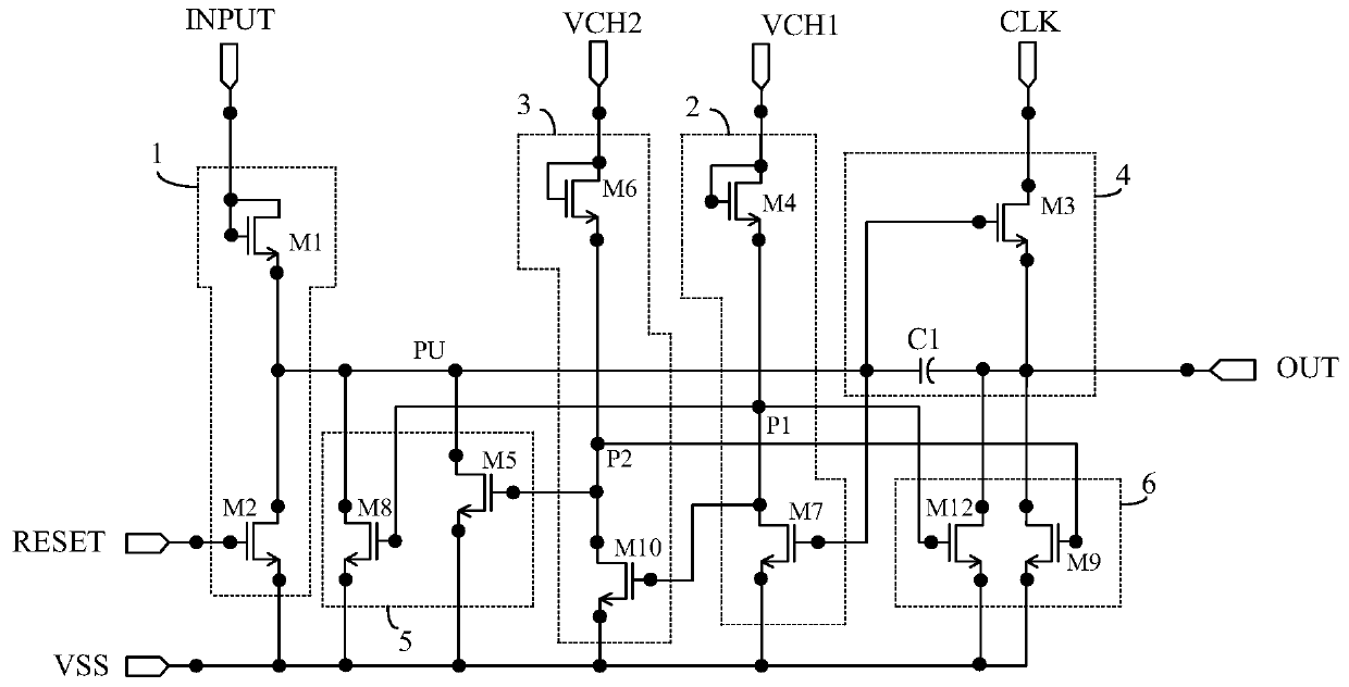
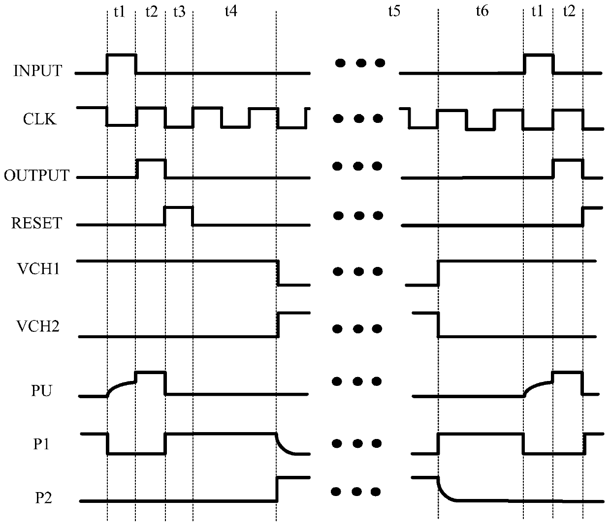
[0063] figure 2 It is a schematic structural diagram of a shift register provided by Embodiment 2 of the present invention, image 3 for figure 2 The working timing diagram of the shift register shown, such as figure 2 and image 3 as shown, figure 2 The shift register shown is based on figure 1 One specific implementation of the shift register shown.

[0064] Optionally, the first pull-down control module 2 includes: a fourth transistor M4 and a seventh transistor M7; wherein, the control electrode of the fourth transistor M4 is connected to the first electrode of the fourth transistor M4, and the first electrode of the fourth transistor M4 pole is connected to the first variable power supply terminal VCH1, the second pole of the fourth transistor M4 is connected to the first pull-down node P1; the control pole of the seventh transistor M7 is connected to the pull-up node PU, and the first pole of the seventh transistor M7 It is connected with the first pull-down no...

Embodiment 3

[0111] Figure 4 A flow chart of a driving method for a shift register provided in Embodiment 3 of the present invention, such as Figure 4 As shown, wherein, the shift register adopts the shift register provided in the first embodiment or the second embodiment above, and the driving method of the shift register includes:

[0112] Step S1 , the precharge reset module precharges the pull-up node under the control of the precharge signal input from the precharge signal input terminal.

[0113] Step S2 , the pull-up module sends the clock control signal in the clock control signal line to the signal output terminal under the control of the potential of the pull-up node, and the signal output terminal outputs a driving voltage.

[0114] Step S3, the pre-charge reset module resets the pull-up node under the control of the reset signal input by the reset signal input terminal, and the second pull-down module outputs the signal under the control of the potentials of the first pull-d...


PUM


Abstract

The invention discloses a shift register, a driving method thereof, a gate driving circuit and a display device. The shift register comprises a precharging reset module, a first pull-down control module, a second pull-down control module, a first pull-down module, a second pull-down module and a pull-up module. The first pull-down control module is used for controlling potential of a first pull-down node through controlling by the potential of a pull-up node. The second pull-down control module is used for controlling the potential of a second pull-down node through controlling by the potential of a first pull-down node. The first pull-down module is used for performing pull-down on the potential of a pull-up node through controlling by the potentials of the first pull-down node and the second pull-down node. The second pull-down module is used for performing pull-down on the potential of a signal output end through controlling by the potentials of the first pull-down node and the second pull-down node. The shift register provided by the invention can perform individual control on output of the signal output end of the shift register so that driving frequency can be regulated, thereby realizing low-frequency and low-power-consumption driving.

Description

technical field [0001] The invention relates to the field of display technology, in particular to a shift register, a driving method thereof, a gate driving circuit and a display device. Background technique [0002] The basic principle of TFT-LCD (Thin Film Transistor-Liquid Crystal Display, thin film transistor liquid crystal display device) to realize a frame display is to input a square wave of a certain width to each row of pixels sequentially from top to bottom through the gate (Gate) drive. Strobe, and then drive the signal required for each row of pixels through the source (Source) and output from top to bottom in turn. At present, the display device with such a structure is usually made of gate drive circuit and source drive circuit on the glass panel by COF (Chip On Film, chip-on-film) or COG (Chip On Glass, chip directly fixed on the glass) process. However, when the resolution is high, the output of the gate drive circuit and the source drive circuit will increa...

Claims


Application Information

Patent Timeline
Patent Type & Authority Patents(China)
IPC IPC(8): G09G3/36G11C19/28
CPCG09G3/36G09G3/3696G09G2310/0286G11C19/28
Inventor 陈鹏张新霞
Owner BOE TECH GRP CO LTD
Why Eureka
Try Eureka