Array substrate, display panel and display device

A technology of array substrates and substrate substrates, applied in nonlinear optics, instruments, optics, etc., to achieve the effect of improving the problem of light leakage in dark states

Inactive Publication Date: 2017-07-07
XIAMEN TIANMA MICRO ELECTRONICS
View PDF4 Cites 9 Cited by
  • Summary
  • Abstract
  • Description
  • Claims
  • Application Information

AI Technical Summary

Problems solved by technology

[0004] The object of the present invention is to provide an array substrate, a display panel, and a display device, so as to solve the problem of light leakage in the dark state caused by the reflection of data lines existing in the existing display panels and display devices, and improve the visual effect of the display panel

Method used


Image

  • Array substrate, display panel and display device
  • Array substrate, display panel and display device
  • Array substrate, display panel and display device

Examples


Embodiment Construction

[0027] The present invention will be further described in detail below in conjunction with the accompanying drawings and embodiments. It should be understood that the specific embodiments described here are only used to explain the present invention, but not to limit the present invention. In addition, it should be noted that, for the convenience of description, only some structures related to the present invention are shown in the drawings but not all structures.

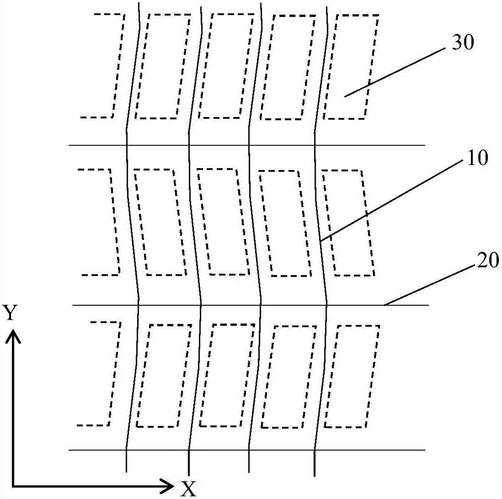
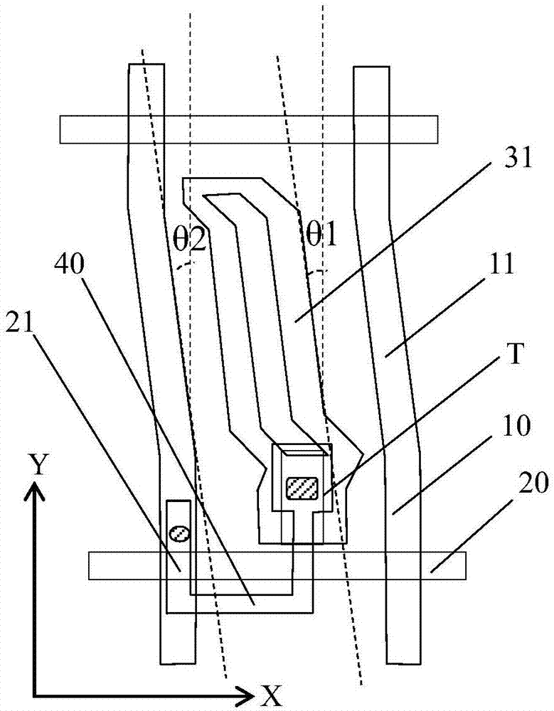
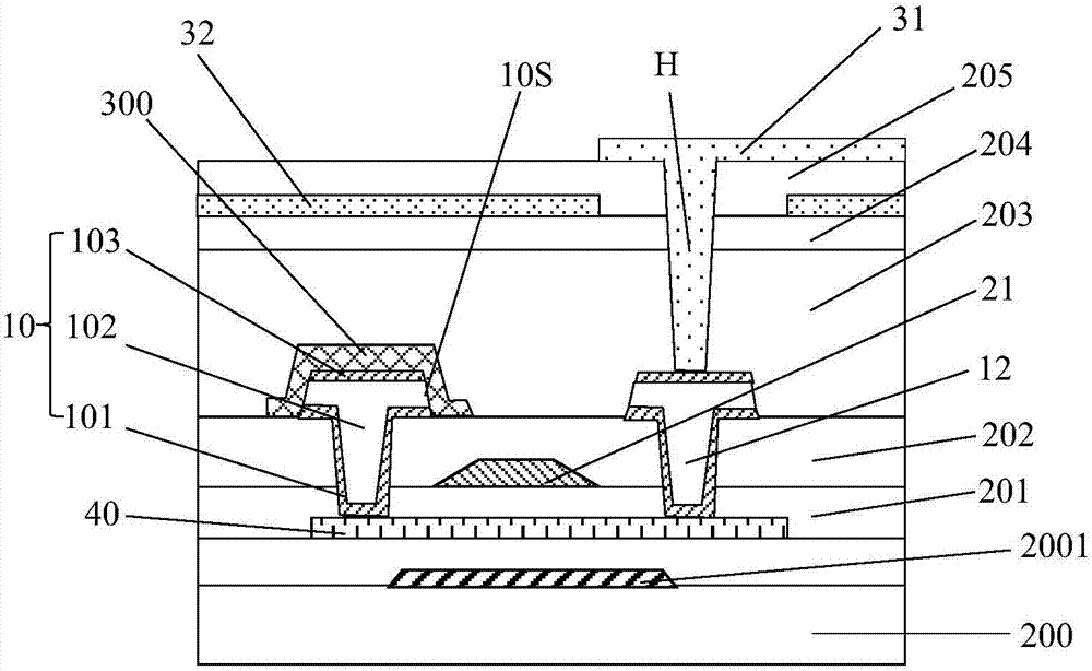
[0028] The present invention provides an array substrate, which sequentially includes: a base substrate; a plurality of scanning lines and a plurality of data lines intersecting to define a plurality of pixel units; a planarization layer covering the plurality of scanning lines and the plurality of data lines, and a low-reflection film layer; wherein the data line includes a first metal layer, and the reflectance of the low-reflection film layer is lower than that of the first metal layer; the low-reflection film l...


PUM

PropertyMeasurementUnit
angleaaaaaaaaaa

Abstract

The invention provides an array substrate, a display panel and a display device. The array substrate comprises a substrate, a plurality of scanning lines, a plurality of data lines, a flattening layer and a low-reflection film layer, wherein the plurality of scanning lines and data lines are positioned on the substrate and provided with a plurality of pixel units in a cross manner; the flattening layer covers the plurality of scanning lines and data lines; and the low-reflection film layer is positioned between the data lines and the flattening layer and covers the data lines. The reflection coefficient of the low-reflection film layer is lower than the reflection coefficient of the data lines. Therefore, the dark-state light leakage problem of the display panel and the display device caused by reflection of the data lines can be effectively improved.

Description

technical field [0001] The present invention relates to the field of display technology, and in particular to an array substrate, a display panel and a display device. Background technique [0002] In the field of liquid crystal display technology, in-plane switching (In-Plane Switching IPS) technology and fringe field switching (Fringe Field Switching FFS) technology are two commonly used wide viewing angle liquid crystal display technologies. With the same substrate, the liquid crystal molecules are rotated in a plane parallel to the substrate, thereby improving the light transmission efficiency of the liquid crystal layer. [0003] A liquid crystal display panel in the prior art usually includes an array substrate and a color filter substrate. Data lines and scan lines are formed on the array substrate, and a plurality of pixel units arranged in a matrix are defined by the data lines and scan lines. The pixel units arranged in a matrix include multiple rows and columns o...

Claims


Application Information

Patent Timeline
Patent Type & Authority Applications(China)
IPC IPC(8): G02F1/1335G02F1/1333G02F1/1362G02F1/1343
CPCG02F1/1333G02F1/133553G02F1/134363G02F1/136286G02F1/133357
Inventor 李元行苏婷陈国照
Owner XIAMEN TIANMA MICRO ELECTRONICS
Why Eureka
Try Eureka