A preparation method and structure of a three-dimensional memory

A memory, three-dimensional technology, applied in the direction of semiconductor devices, electric solid state devices, electrical components, etc., can solve the problems of contact failure, uncontrollable wafer stress, contact hole 17 growth, etc., to reduce wafer bending and improve macroscopic stress. The effect of distribution

Active Publication Date: 2019-01-29
YANGTZE MEMORY TECH CO LTD
View PDF3 Cites 0 Cited by
  • Summary
  • Abstract
  • Description
  • Claims
  • Application Information

AI Technical Summary

Problems solved by technology

Based on the existing manufacturing process of three-dimensional memory, when the number of stacked layers of memory cells increases, the thickness of the dielectric layer of the required peripheral circuit will increase. In the subsequent process, heat treatment makes the stress of the wafer uncontrollable. , the wafer becomes bent under the stress of thicker silicon dioxide. When the wafer is bent to a certain extent, it not only brings about the problem of overlay accuracy of the mask, but also affects the ability of the manipulator to grab the wafer; The three-dimensional memory chip is divided into an array storage area 12 and a peripheral circuit area 11. During the preparation of the array storage area 12, due to the inhomogeneity of local stress, the peripheral circuit area 11 is squeezed, so that when the contact hole 17 is formed, the contact Hole 17 cannot grow within the contact window of the device completely according to the design intention, resulting in contact failure

Method used


Image

  • A preparation method and structure of a three-dimensional memory
  • A preparation method and structure of a three-dimensional memory
  • A preparation method and structure of a three-dimensional memory

Examples


Embodiment 1

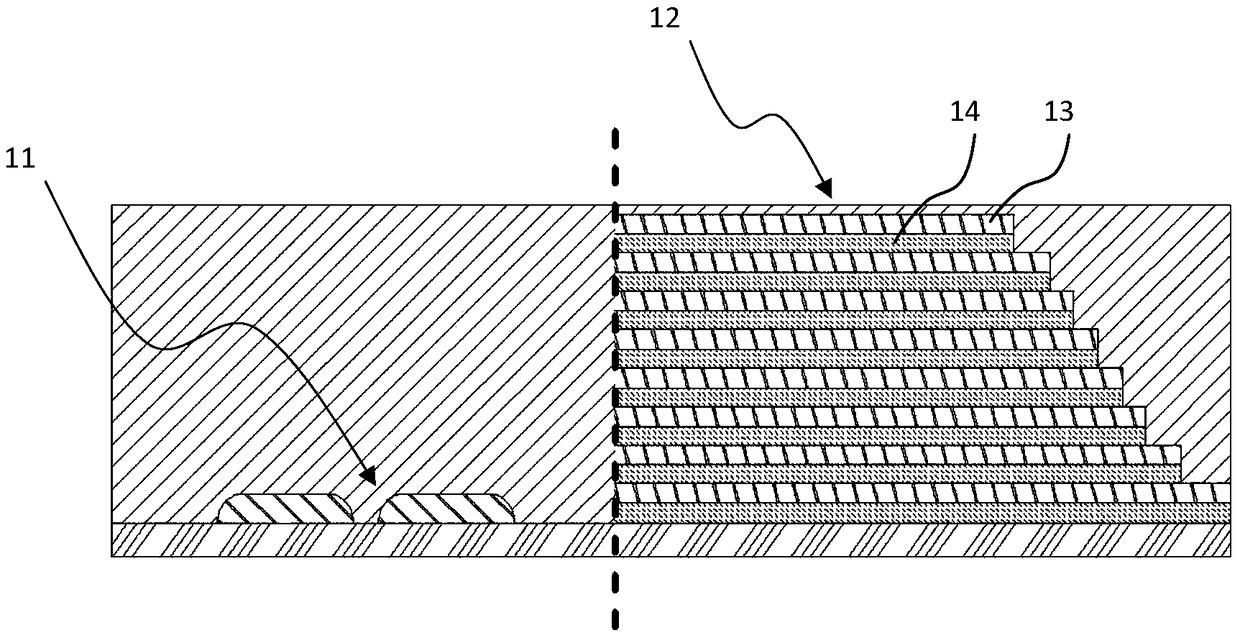
[0030] refer to Figure 5-10 As shown, Embodiment 1 of the present invention proposes a method for preparing a three-dimensional memory, which is characterized in that it includes the following steps:

[0031] Such as Figure 5 As shown, a substrate 20 is provided, on which a peripheral circuit area 21 and an array storage area 22 of a three-dimensional memory are formed; preferably, forming the array storage area 22 includes alternately forming silicon nitride on the substrate 20 A multilayer stack structure of layer 23 and silicon oxide layer 24; using a photolithography process to form a step region 25 on at least one side of the multilayer stack structure so that a part of the upper surface of each silicon nitride layer 23 is exposed to the step region 25.

[0032] Forming an insulating layer 26 with a flat surface on the substrate 20 to cover the peripheral circuit area 21 and the array storage area 22;

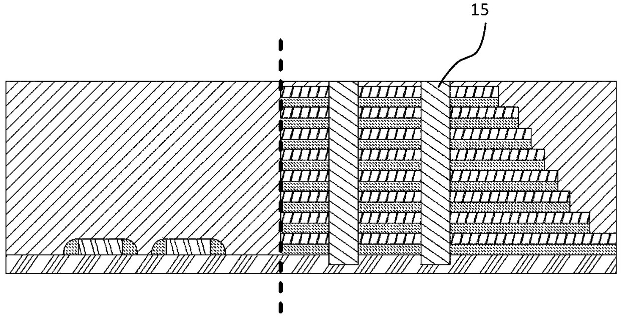
[0033] Such as Image 6 As shown, the insulating layer 26 on th...

Embodiment 2

[0038] Embodiment 2 of the present invention proposes a method for preparing a three-dimensional memory, which is characterized in that it includes the following steps:

[0039] Such as Image 6As shown, preferably, after the insulating layer 26 on the peripheral circuit region 21 is patterned, etched and filled with metal to form a plurality of first contact holes 27 electrically connected to the peripheral circuit region 21, It also includes the step of performing a chemical mechanical mask on the surface of the substrate 20 .

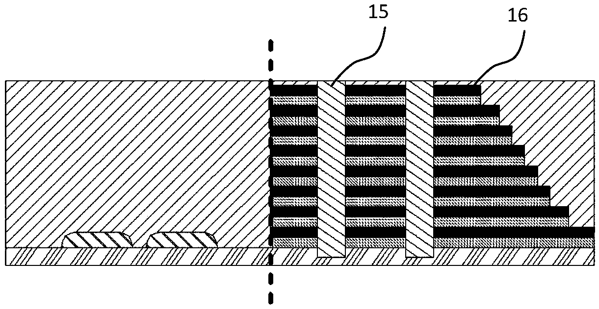
[0040] Such as Figure 7 As shown, preferably, after the step of performing a chemical mechanical mask on the surface of the substrate 20, a step of depositing a silicon dioxide cap layer 31 on the substrate 20 is also included to protect the first contact hole 27 The metal fill in is not damaged by subsequent processes.

[0041] Preferably, the thickness of the silicon dioxide cap layer is greater than 3000 angstroms.

Embodiment 3

[0043] Embodiment 3 of the present invention proposes a method for manufacturing a three-dimensional memory. In this embodiment, parts different from those in the above embodiments will be described, and the same parts will not be described again.

[0044] Such as Figure 9 As shown, preferably, after forming the metal gate 29 of the memory cell in the array storage area 22 , a step of depositing a silicon dioxide filling layer 32 on the silicon dioxide cap layer 31 is also included.


PUM


Abstract

The preparation method and structure of a three-dimensional memory provided by the present invention, by advancing the contact hole process in the peripheral circuit area before the memory cell channel process in the array storage area, the etching of the contact hole can affect the silicon dioxide film in the peripheral circuit area. The release of stress improves the macroscopic stress distribution of the wafer and effectively reduces bending. In addition, since the contact holes in the peripheral circuit area are placed before the channel process of the memory cell in the array storage area, the metal gate process of the array storage area and the channel process of the array storage area Local stress inhomogeneity will not cause contact failure of peripheral circuits.

Description

technical field [0001] The invention relates to the field of semiconductor devices and their manufacture, in particular to a preparation method and structure of a three-dimensional memory. Background technique [0002] With the continuous improvement of market demand for memory capacity, the number of memory cells that can be provided per unit area by traditional memory based on planar or two-dimensional structures is approaching the limit, which cannot further meet the market demand for larger capacity memory. Just like several bungalows built on a limited plane, these bungalows are neatly arranged, but as the demand continues to increase, the number of bungalows continues to blow out, but in the end this limited plane can only accommodate a certain number of bungalows. Cannot continue to increase. Planar memory is approaching its practical expansion limit, which brings severe challenges to the semiconductor memory industry. [0003] In order to solve the above difficulti...

Claims


Application Information

Patent Timeline
Patent Type & Authority Patents(China)
IPC IPC(8): H01L27/11582H01L27/11573H01L27/11556H01L27/11531
CPCH10B41/42H10B41/27H10B43/40H10B43/27
Inventor 宋豪杰徐强李广济邵明夏志良霍宗亮
Owner YANGTZE MEMORY TECH CO LTD
Why Eureka
Try Eureka