Five-point recognition method for CCDs (Charge Coupled Devices)

A mid-point, PCB board technology, applied in the direction of optical testing flaws/defects, measuring devices, instruments, etc., can solve the problems of test FAIL, the product cannot be attached to the PAD, etc., and achieve the effect of improving the pass rate

Active Publication Date: 2017-12-29
SHENZHEN MASONE ELECTRONICS
View PDF7 Cites 4 Cited by
  • Summary
  • Abstract
  • Description
  • Claims
  • Application Information

AI Technical Summary

Problems solved by technology

[0003] The purpose of the present invention is to provide a five-point identification CCD method for the technical problems existing in the prior art, which can solve the problem that when the PCB board is tested, the overall offset or rotating product cannot be stuck on the PAD, resulting in a test FAIL problem

Method used


Image

  • Five-point recognition method for CCDs (Charge Coupled Devices)
  • Five-point recognition method for CCDs (Charge Coupled Devices)
  • Five-point recognition method for CCDs (Charge Coupled Devices)

Examples


Embodiment Construction

[0028] In order to facilitate the understanding of the present invention, the present invention will be described more fully below with reference to the associated drawings. Preferred embodiments of the invention are shown in the accompanying drawings. However, the present invention can be embodied in many different forms and is not limited to the embodiments described herein. Rather, these embodiments are provided for the purpose of making the disclosure of the present invention more thorough and comprehensive.

[0029] Unless otherwise defined, all technical and scientific terms used herein have the same meaning as commonly understood by one of ordinary skill in the technical field of the invention. The terms used herein in the description of the present invention are for the purpose of describing specific embodiments only, and are not intended to limit the present invention.

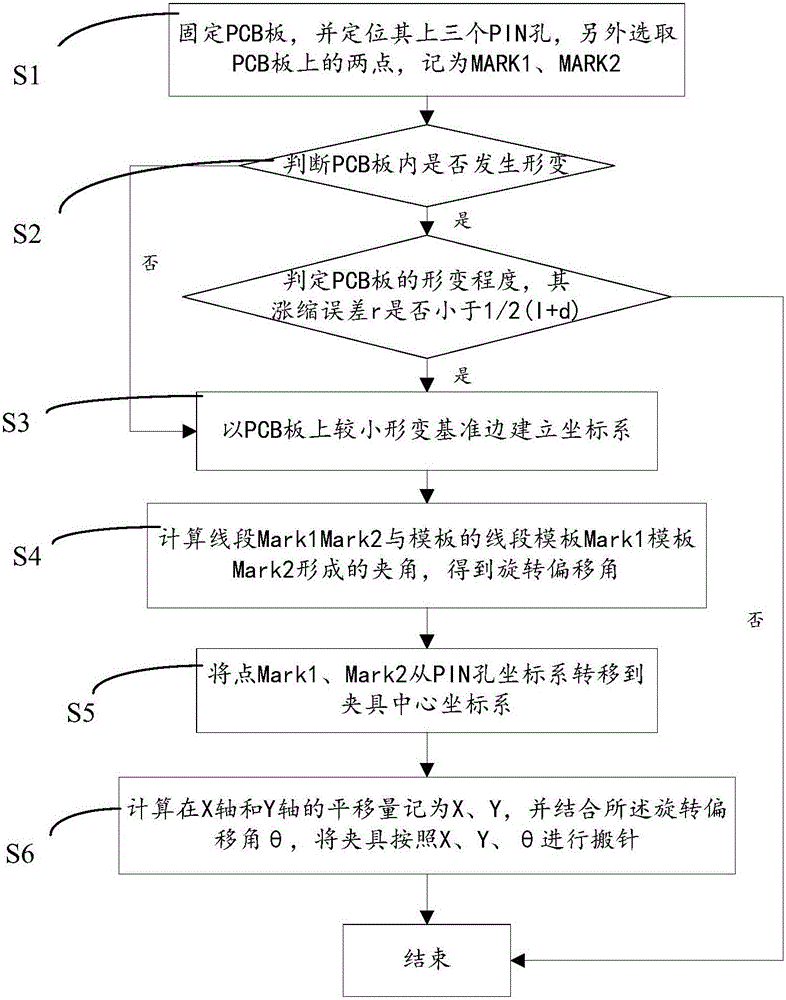
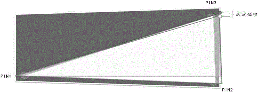
[0030] refer to figure 1 As shown, a kind of five-point recognition CCD method provided by the ...


PUM


Abstract

The invention discloses a five-point recognition method for CCDs (Charge Coupled Devices). The method includes the following steps that: a PCB (printed circuit board) is fixed, three PIN holes on the PCB are positioned, two addition points are selected from the PCB and marked as MARK1 and MARK2 respectively; whether deformation occurs in the PCB is judged through judging whether the triangle of the PIN holes of the PCB is totally equal to the triangle of the PIN holes of a template, if no deformation occurs in the PCB or the expansion and shrinkage error r of the PCB is smaller than 1/2 (l+d), a coordinate system is built with a small-deformation reference edge of the PCB, namely, the opposite side of the smallest-deformation angle of the PCB is adopted as an X axis, and a PIN hole coordinate system is built with one endpoint or the middle point of the side adopted as an origin point; an included angle between a ling segment Mark1Mark2 and a line segment template Mark1 and template Mark2 is calculated, so that a rotation shift angle is obtained; the point Mark1 and point Mark2 are shifted to a fixture center coordinate system from the PIN hole coordinate system; and the translation quantities of the PCB on an X axis and a Y axis are recorded as X and Y respectively, and a fixture (or the PCB) is made to move according to X, Y and Theta (or -X,-Y and -Theta) on the basis of the rotation shift angle. The recognition method of the present invention is more accurate and more stable.

Description

technical field [0001] The present invention relates to the technical field of machine vision, and more specifically, relates to a five-point recognition CCD method. Background technique [0002] CCD systems are traditionally used in PCB testing equipment, using two-point or four-point markings for analysis. Among them, the two-point marking method requires high positioning consistency between the CCD station and the fixture test station, which is often difficult to achieve. Due to the offset of the positioning reference, the analysis will be biased, which will easily cause the CCD system to be ineffective. Using the four-point marking method is more accurate, but often there will be damage to the PIN hole, and a single PIN hole will be displaced, resulting in the lack of a benchmark for the four-point analysis system, which naturally makes the analysis inaccurate, and the CCD effect is naturally unsatisfactory. Contents of the invention [0003] The purpose of the presen...

Claims


Application Information

Patent Timeline
Patent Type & Authority Applications(China)
IPC IPC(8): G01B11/16G01N21/95
Inventor 徐谨慎高云峰
Owner SHENZHEN MASONE ELECTRONICS
Why Eureka
Try Eureka