

Pixel structure, array substrate and display panel
A technology of pixel structure and array substrate, applied in nonlinear optics, instruments, optics, etc., can solve the problems of voltage-stabilizing line potential jump difference amplification, horizontal crosstalk, etc., and achieve the effect of eliminating discharge
- Summary
- Abstract
- Description
- Claims
- Application Information
AI Technical Summary
Problems solved by technology
Method used
Image

Examples
Embodiment Construction
[0013] Certain words are used to refer to specific components in the description and claims, and those skilled in the art should understand that manufacturers may use different terms to refer to the same component. The specification and claims do not use the difference in name as a way to distinguish components, but use the difference in function of components as a basis for distinction. The present invention will be described in detail below in conjunction with the accompanying drawings and embodiments.
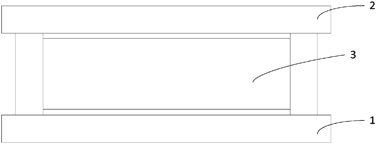
[0014] figure 1 is a schematic structural diagram of a display panel according to an embodiment of the present invention. Such as figure 1 As shown, the display panel includes an array substrate 1 , an opposite substrate 2 disposed opposite to the array substrate 1 , and a liquid crystal layer 3 sandwiched between the array substrate 1 and the opposite substrate 2 . Wherein, the opposite substrate 2 may be a color filter substrate in a display panel.
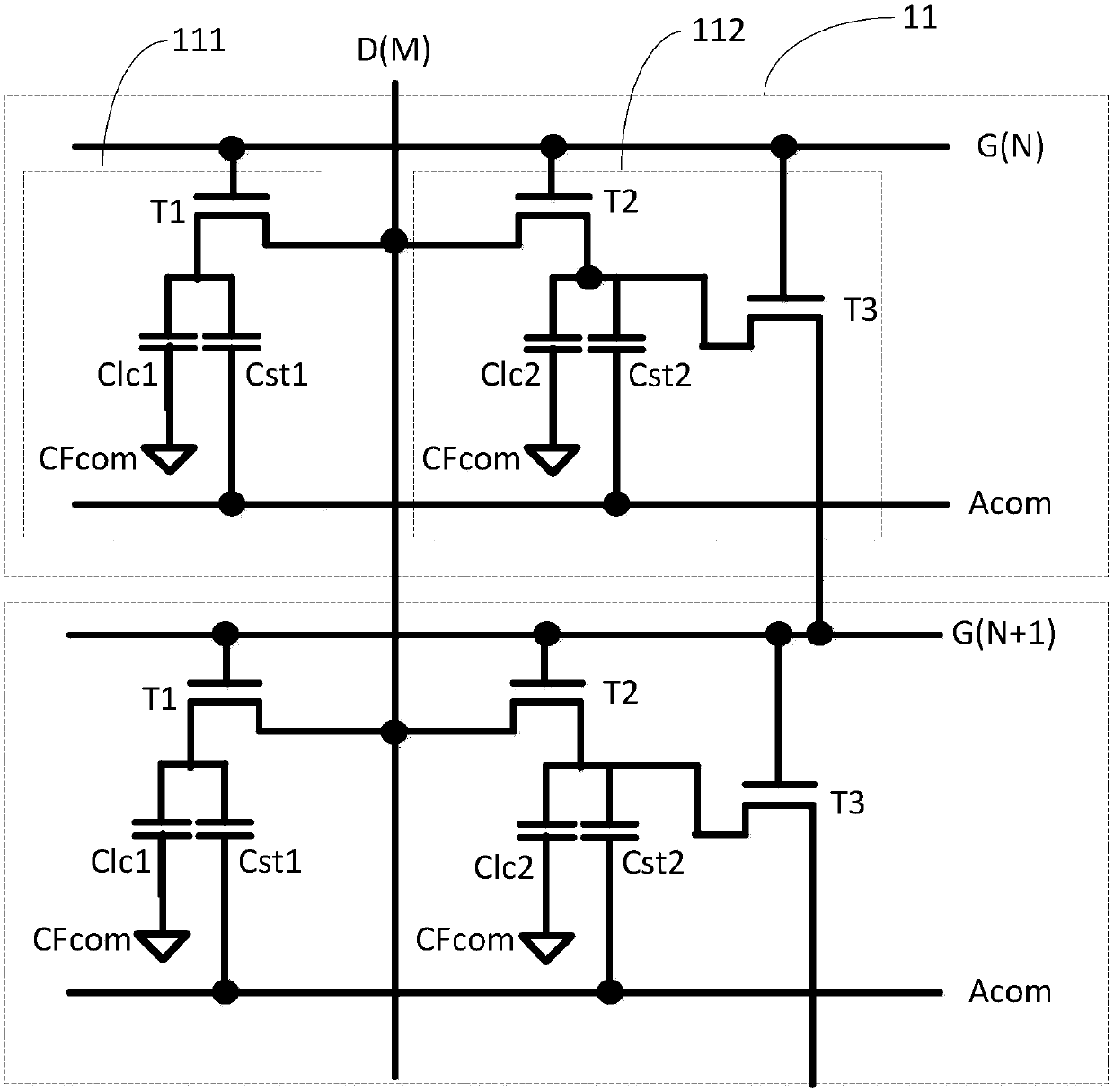
[0015] figure 2 ...
PUM
 Abstract
Description
Claims
Application Information