Array substrate and preparation method thereof, and display device

A technology of array substrates and substrate substrates, which is applied in semiconductor/solid-state device manufacturing, semiconductor devices, electrical components, etc. It can solve the problems of different oxygen-containing environments and difficulty in balancing the stability of multiple thin film transistors at the same time

Active Publication Date: 2018-05-15
BOE TECH GRP CO LTD
View PDF3 Cites 11 Cited by
  • Summary
  • Abstract
  • Description
  • Claims
  • Application Information

AI Technical Summary

Problems solved by technology

[0004] Embodiments of the present invention provide an array substrate, a preparation method thereof, and a display device, which can solve the problem that multiple thin film transistors in an existing array substrate have different oxygen-containing environments due to different application requirements, and it is difficult to balance the work of multiple thin film transistors at the same time. problem of stability

Method used


Image

  • Array substrate and preparation method thereof, and display device
  • Array substrate and preparation method thereof, and display device
  • Array substrate and preparation method thereof, and display device

Examples


Embodiment Construction

[0035] The technical solutions in the embodiments of the present invention will be clearly and completely described below in conjunction with the accompanying drawings in the embodiments of the present invention. Obviously, the described embodiments are only a part of the embodiments of the present invention, rather than all the embodiments. Based on the embodiments of the present invention, all other embodiments obtained by those of ordinary skill in the art without creative work shall fall within the protection scope of the present invention.

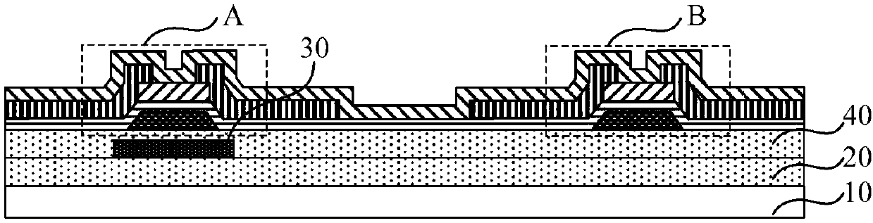
[0036] The embodiment of the present invention provides an array substrate, such as figure 1 As shown, it includes a base substrate 10, and also includes a first buffer layer 20, an oxygen barrier pattern 30, and a second buffer layer 40 sequentially disposed on the base substrate 10, and a first film disposed on the second buffer layer 40 For the transistor A and the second thin film transistor B, the orthographic projection of the chann...


PUM


Abstract

The embodiments of the invention provide an array substrate and a preparation method thereof and a display device, which relate to the technical field of display. The problem that the multiple thin film transistors in the existing array substrate need different oxygen-bearing environments because of different application needs and it is difficult to balance the working stability of the thin film transistors at the same time can be solved. The array substrate includes a base substrate, and further includes a first buffer layer, an oxygen barrier pattern and a second buffer layer arranged on thebase substrate in sequence, and a first thin film transistor and a second thin film transistor arranged on the second buffer layer. The orthographic projection of the channel region of the first thinfilm transistor on the base substrate falls within the boundary range of the orthographic projection of the oxygen barrier pattern on the base substrate. The oxygen content of the first buffer layeris higher than that of the second buffer layer.

Description

Technical field [0001] The present invention relates to the field of display technology, in particular to an array substrate, a preparation method thereof, and a display device. Background technique [0002] Compared with the conventional back-channel etched (BCE) and etch-stopped (ESL) thin film transistors, the top-gate structure oxide thin film transistor has the following advantages: significantly reduces parasitic capacitance and is more conducive to achieving good driving Effect; can reduce the production size, which is more conducive to achieving high-resolution display requirements; can reduce the thickness of the gate insulating layer, which is conducive to further reducing the overall production thickness; can achieve more stable electrical characteristics of thin film transistors, thereby Improve the reliability of the display panel. [0003] For the driving thin film transistor (Driving TFT) and the switching thin film transistor (SwitchTFT) that realize different func...

Claims


Application Information

Patent Timeline
Patent Type & Authority Applications(China)
IPC IPC(8): H01L27/12H01L21/77
CPCH01L27/1218H01L27/1225H01L27/1262H01L29/78633H01L29/7869H01L29/78603H10K59/126H10K59/1201
Inventor 顾鹏飞
Owner BOE TECH GRP CO LTD
Why Eureka
Try Eureka