
A silicon carbide semiconductor component

A semiconductor and silicon carbide technology, applied in the field of silicon carbide semiconductor components, can solve the problem of high on-resistance and achieve the effect of reducing the on-resistance ratio

Active Publication Date: 2021-07-23
SHANGHAI HESTIA POWER INC
View PDF5 Cites 0 Cited by
  • Summary
  • Abstract
  • Description
  • Claims
  • Application Information

AI Technical Summary

Problems solved by technology

[0007] The main purpose of the present invention is to solve the problem of relatively high on-resistance caused by sacrificing part of the channel width in the silicon carbide semiconductor component integrating JBS diodes in the prior art

Method used


Image

  • A silicon carbide semiconductor component
  • A silicon carbide semiconductor component
  • A silicon carbide semiconductor component

Examples


Embodiment approach

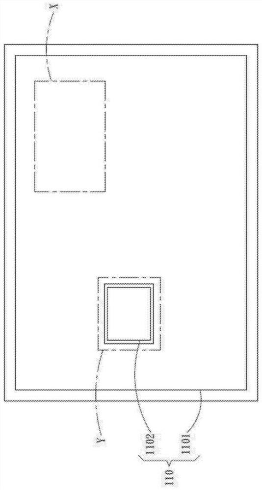
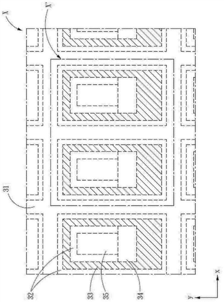
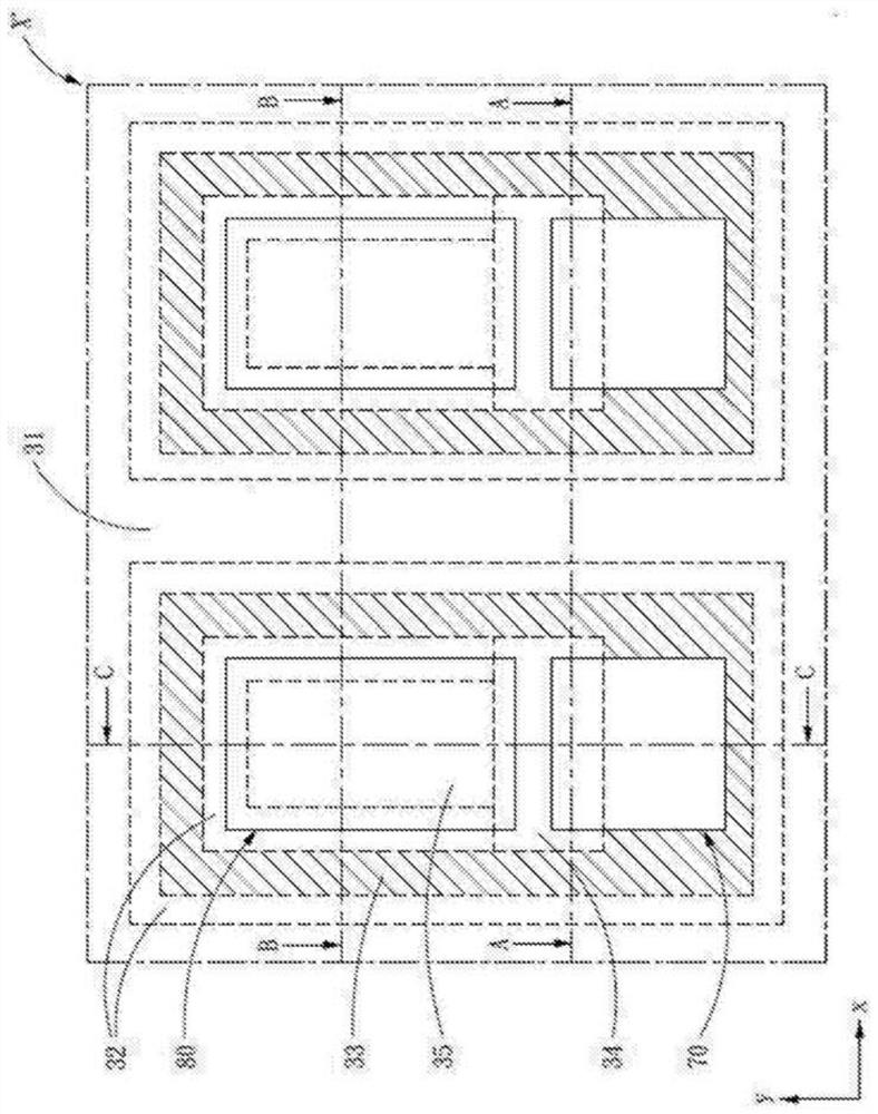
[0031] Related to the detailed description and technical contents of the present invention, now in conjunction with the accompanying drawings are described as follows: Figure 1 to Figure 3B They are respectively the schematic top view of the silicon carbide semiconductor component of the present invention, and the figure 1 The enlarged schematic diagram of the X area in the Figure 2A The enlarged schematic diagram of the X’ area in Figure 2B A-A cross-sectional schematic diagram in Figure 2B The B-B cross-sectional schematic diagram in Figure 2B The C-C sectional schematic diagram in, the embodiment of the present invention is in figure 1 The zoomed-in schematic diagram of the Y area in and Figure 3A Schematic diagram of the D-D section in . Such as Figure 1 to Figure 3B As shown, a silicon carbide semiconductor component of the present invention includes a substrate 10, an n-type drift layer 20, a plurality of doped regions 30, a gate dielectric layer 40, a gate ...


PUM

PropertyMeasurementUnit
electrical resistivityaaaaaaaaaa
thicknessaaaaaaaaaa
thicknessaaaaaaaaaa

Abstract

A silicon carbide semiconductor component, using a silicon carbide substrate to form an integrated structure, the integrated structure has a metal oxide semiconductor field effect transistor and a junction barrier Schottky reverse parallel connection of the metal oxide semiconductor field effect transistor diode.

Description

【Technical field】 [0001] The invention relates to a silicon carbide semiconductor component, in particular to a silicon carbide semiconductor component with a low on-resistance ratio. 【Background technique】 [0002] In terms of the characteristics of semiconductor power components, it is required to have the minimum on-resistance, low reverse leakage current and fast switching speed in order to reduce the conduction loss during operation. And switching loss (Switching loss). Silicon carbide (SiC for short) is considered to be the Excellent material for power switching components. Under the same breakdown voltage condition, the thickness of the withstand voltage layer (drift layer with low doping concentration) of power components made of silicon carbide is only one tenth of the thickness of silicon (Si) power components. One; and the theoretical on-resistance can reach one hundredth of that of silicon. [0003] However, due to the wide energy gap of silicon carbide, the ...

Claims


Application Information

Patent Timeline
Patent Type & Authority Patents(China)
IPC IPC(8): H01L29/78H01L29/06H01L29/16
CPCH01L29/0684H01L29/0696H01L29/1608H01L29/7828
Inventor 颜诚廷洪建中李传英
Owner SHANGHAI HESTIA POWER INC
Learn More