
Method for preparing diamond abrasive material tool with orderly distributed abrasive particles by utilizing mask
A diamond and mask technology, which is used in manufacturing tools, grinding devices, metal processing equipment, etc., can solve the problem that the orderly arrangement of diamond abrasive grains is poor in craftsmanship, and it is difficult to achieve single-layer brazing of fine-grained diamond abrasives. Soldering and brazing bonding agent layer thickness and other problems, to achieve the effect of good exposure height consistency, conducive to mass production, and simple equipment
- Summary
- Abstract
- Description
- Claims
- Application Information
AI Technical Summary
Problems solved by technology
Method used
Image


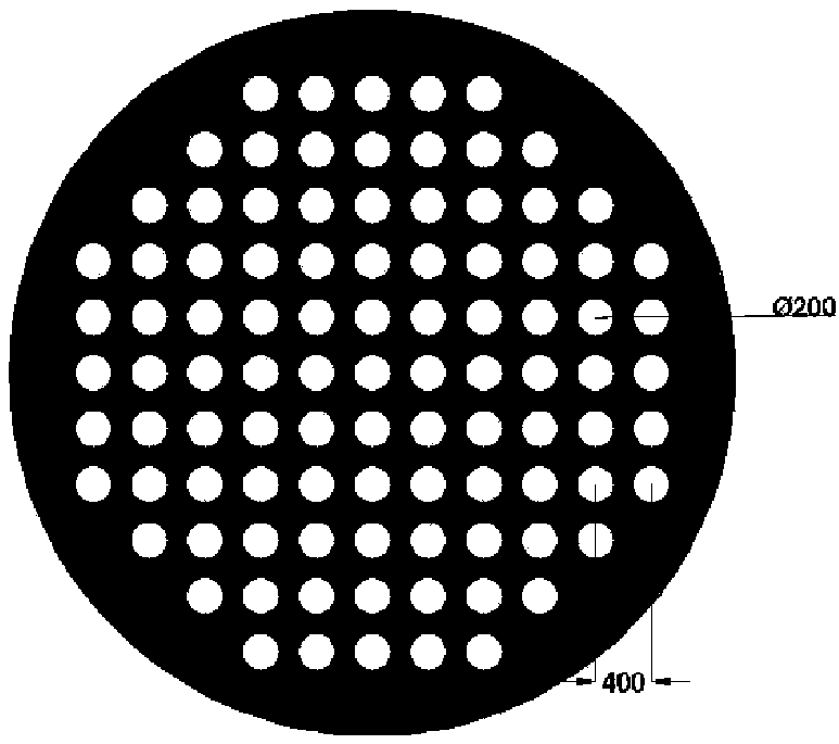
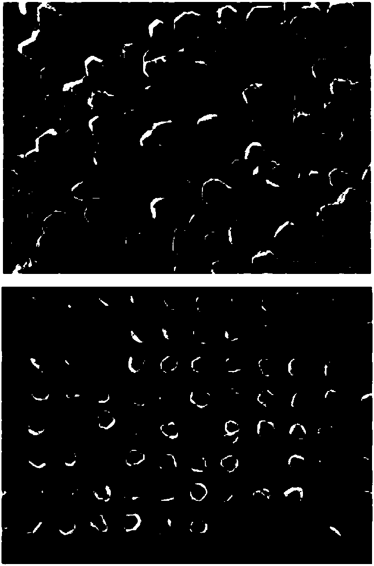
Examples
Embodiment 1
[0044] The substrate is silicon carbide ceramics, the abrasive is 100-mesh diamond powder, the thickness of the mask plate is 150 μm, and the surface is etched with a matrix-shaped through-hole array arranged in an orderly manner, and the diameter of the through-hole is 200 μm.
[0045] The surface of the substrate was ground with 15 μm diamond micropowder for 1 min, and then the substrate was ultrasonically cleaned with acetone. Then coat the photoresist on the surface of the substrate, and stick the mask on the surface of the substrate. Then, the diamond powder is spread on the mask, and the substrate is fully vibrated, so that each hole of the mask is filled with a single diamond grain. The excess diamond grit is then wiped off and the mask is removed. The orderly arranged diamond abrasive grains are fixed on the surface of the substrate. Then, the diamond coating is deposited on the surface of the substrate by hot wire chemical vapor deposition equipment, and the abrasiv...
Embodiment 2
[0050] The substrate is cemented carbide, the abrasive is 100-mesh diamond powder, the thickness of the mask plate is 150 μm, and the surface is etched with a matrix-shaped through-hole array arranged in an orderly manner, and the diameter of the through-hole is 200 μm.
[0051] The cemented carbide substrate is pretreated with acid and alkali, and the cemented carbide substrate is first immersed in Murakami solution (10g K 3 [Fe(CN)] 6 +10g KOH+100mL H 2 O) in ultrasonic treatment for 30min, then soak it in mixed acid (HCl: H 2 o 2 =1:3) for 1 minute to remove the cobalt element on the surface, and then clean the surface of the substrate with acetone. Then coat the photoresist on the surface of the substrate, and stick the mask on the surface of the substrate. Then the diamond powder is spread on the mask, and the tool substrate is fully vibrated, so that each hole of the mask is filled with a single diamond grain. The excess diamond grit is then wiped off and the mask i...
Embodiment 3
[0054] The substrate is silicon carbide, the abrasive is 170-mesh diamond powder, the thickness of the mask is 100 μm, and the surface is etched with a matrix-shaped through-hole array arranged in an orderly manner, the diameter of the through-holes is 100 μm, and the spacing is 200 μm.
[0055] The surface of the substrate was ground with 15 μm diamond powder for 1 min, and then the substrate was ultrasonically cleaned with acetone. Then coat the photoresist on the surface of the substrate, and stick the mask on the surface of the substrate. Then, the diamond powder is spread on the mask, and the substrate is fully vibrated, so that each hole of the mask is filled with a single diamond grain. The excess diamond grit is then wiped off and the mask is removed. The orderly arranged diamond abrasive grains are fixed on the surface of the substrate. Then, the diamond coating is deposited on the surface of the substrate by hot wire chemical vapor deposition equipment, and the abr...
PUM
| Property | Measurement | Unit |
|---|---|---|
| particle diameter | aaaaa | aaaaa |
| particle diameter | aaaaa | aaaaa |
| thickness | aaaaa | aaaaa |
Abstract
Description
Claims
Application Information