Writing film structure and projection writing device produced by same
A writing device and layer structure technology, applied in the field of projection and writing, can solve problems such as the inability to realize projection display
- Summary
- Abstract
- Description
- Claims
- Application Information
AI Technical Summary
Problems solved by technology
Method used
Image

Examples
Embodiment 1
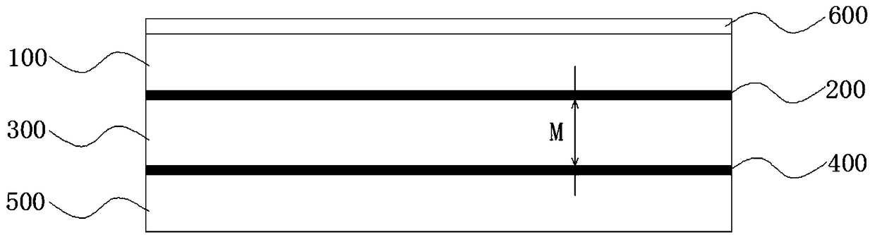
[0039] Such as figure 1 As shown, the first embodiment provides a writing film layer structure, including: the first base layer 100, the first conductive layer 200, the liquid crystal layer 300, the second conductive layer 400 and the second base layer 500 arranged in sequence, the second The second base layer 500 is a transparent base material.
[0040] In the writing film layer structure, the liquid crystal layer 300 containing liquid crystal such as liquid crystal microdroplets 310 is filled between the first conductive layer 200 and the second conductive layer 400 as the writing substrate, because the material has a reflective state and a scattering state All are stable-state characteristics, so that the user can write freely on the writing film layer; and, since the second matrix layer 500 in the writing film layer is set as a transparent substrate, the setting of the transparent substrate makes the The writing film layer structure presents a transparent or translucent s...
Embodiment 2
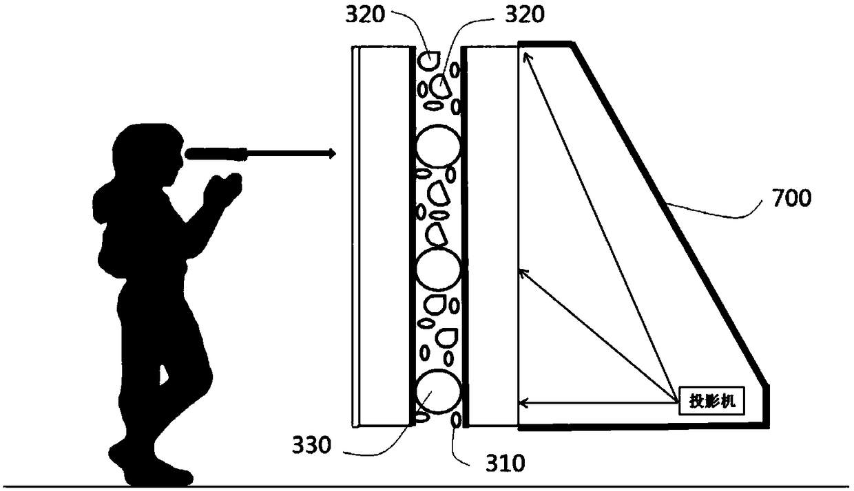
[0060] Such as figure 1 and 2 As shown, the present embodiment 2 provides a projection writing device including: a projection module and a display screen, the display screen includes the writing film layer structure in the above embodiment 1; the projection module projects the projection information onto the display screen by means of rear projection .
[0061] The projection writing device is manufactured by using the writing film layer structure in the first embodiment above, wherein the specific structure and beneficial effects of the writing film layer structure have been described in detail in the above text, and will not be repeated here.
[0062] Wherein, an electric control board is provided between the first conductive layer 200 and the second conductive layer 400 to control the power state between the first conductive layer 200 and the second conductive layer 400 .
[0063] Such as figure 2 As shown, the projection module includes a projector and a black curtain ...
PUM
| Property | Measurement | Unit |
|---|---|---|
| Particle size | aaaaa | aaaaa |
Abstract
Description
Claims
Application Information
 - R&D
- Intellectual Property
- Life Sciences
- Materials
- Tech Scout
- Unparalleled Data Quality
- Higher Quality Content
- 60% Fewer Hallucinations
Browse by: Latest US Patents, China's latest patents, Technical Efficacy Thesaurus, Application Domain, Technology Topic, Popular Technical Reports.
© 2025 PatSnap. All rights reserved.Legal|Privacy policy|Modern Slavery Act Transparency Statement|Sitemap|About US| Contact US: help@patsnap.com