A method for processing the shape of a micro-sized pcb board

A PCB board and shape processing technology, which is applied in the fields of printed circuit, electrical components, printed circuit manufacturing, etc., can solve the problems that the board cannot be machined, has no processing technology, carbon black, etc., and achieves the effect of improving product yield and ensuring precision

Active Publication Date: 2021-04-16
珠海杰赛科技有限公司 +1
View PDF11 Cites 0 Cited by
  • Summary
  • Abstract
  • Description
  • Claims
  • Application Information

AI Technical Summary

Problems solved by technology

[0002] At present, in the field of PCB board processing, mechanical CNC milling or laser milling is used for shape processing. Mechanical milling is milling through the milling cutter of the CNC machine tool, and processing chips will be generated during the processing. Chips therefore need to be equipped with a vacuum tube, so the mechanical edge milling is affected by the diameter of the milling cutter, the diameter of the vacuum tube and the milling path; the general dimensions of the processed PCB need to be greater than or equal to 5mm*1mm (length*width), for less than this The size of the board cannot be machined; the laser milling method is restricted by the thickness of the board, and generally can only process PCB boards less than or equal to 0.8mm. For boards with a thickness exceeding 0.8mm, serious carbon black will be produced and cannot be used legally.
Therefore, there is currently no corresponding processing technology for plates with a thickness greater than 0.8mm and a size less than 5mm*1mm

Method used


Image

  • A method for processing the shape of a micro-sized pcb board

Examples


Embodiment Construction

[0014] In order to make the object, technical solution and advantages of the present invention clearer, the present invention will be further described in detail in conjunction with the accompanying drawings and embodiments. It should be understood that the specific embodiments described here are only used to explain the present invention, and are not limited to the present invention.

[0015] The present invention is described in further detail below in conjunction with accompanying drawing embodiment:

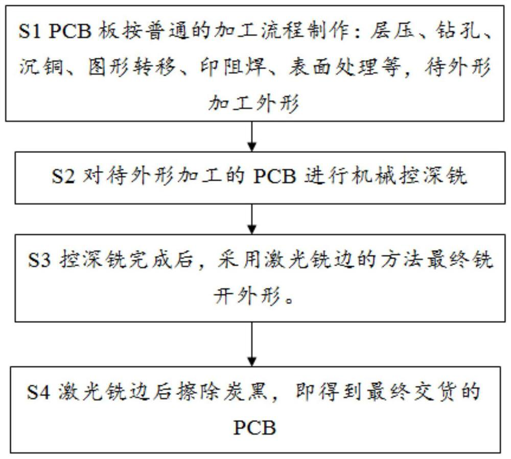
[0016] like figure 1 Shown: a method for processing the shape of a micro-sized PCB board, the processing method includes the following steps:

[0017] Step 1: Provide a pre-processed PCB board to be processed; the PCB board undergoes a series of processing procedures: lamination, drilling, copper sinking, pattern transfer, printing and solder mask, and surface treatment to ensure that all processes are in normal operation , so that the quality and size of the PCB board can ...


PUM


Abstract

A method for processing the shape of a micro-sized PCB board, comprising the following four steps: Step 1: providing a pre-treated PCB board to be processed; Step 2: mechanically controlling the PCB board to be processed in the first step Deep milling; Step 3: Laser edge milling the PCB board processed in Step 2; Step 4: Erase carbon black on the PCB board processed in Step 3. The invention adopts the processing method of "mechanical numerical control edge milling + laser edge milling", which makes up for the processing defects of the prior art for PCB boards with a thickness greater than 0.8mm and a size less than 5mm*1mm, which not only ensures the processing accuracy, but also improves It not only improves the product yield, but also ensures that the product meets the quality and performance requirements, and has the advantages of high efficiency and high precision.

Description

【Technical field】 [0001] The invention relates to the field of PCB board processing, in particular to a method for processing the shape of a micro-sized PCB board. 【Background technique】 [0002] At present, in the field of PCB board processing, mechanical CNC milling or laser milling is used for shape processing. Mechanical milling is milling through the milling cutter of the CNC machine tool, and processing chips will be generated during the processing. Chips therefore need to be equipped with a vacuum tube, so the mechanical edge milling is affected by the diameter of the milling cutter, the diameter of the vacuum tube and the milling path; the general dimensions of the processed PCB need to be greater than or equal to 5mm*1mm (length*width), for less than this The size of the board cannot be machined; the laser milling method is restricted by the thickness of the board, and generally can only process PCB boards less than or equal to 0.8mm. For boards with a thickness exc...

Claims


Application Information

Patent Timeline
Patent Type & Authority Patents(China)
IPC IPC(8): H05K3/00
CPCH05K3/00
Inventor 刘国汉黄德业关志锋
Owner 珠海杰赛科技有限公司
Why Eureka
Try Eureka