Blind hole circuit board and manufacturing method thereof

A manufacturing method and circuit board technology, which is applied in multilayer circuit manufacturing, printed circuit manufacturing, printed circuit, etc., can solve the problems affecting the thickness control of finished boards, the difficulty of controlling the copper grinding of holes, and the thickness of finished boards exceeding the standard, etc., to achieve Avoid excessive plate thickness, improve line gap production capacity, and facilitate control

Active Publication Date: 2019-03-01
广东依顿电子科技股份有限公司
View PDF12 Cites 2 Cited by
  • Summary
  • Abstract
  • Description
  • Claims
  • Application Information

AI Technical Summary

Problems solved by technology

However, in the plating process, the plating process needs to make a plated film one more time, and then plate the hole, remove the film and grind away the copper protruding from the hole when the hole is plated. The process is cumbersome and the copper grinding of the hole is difficult to control, making the production cost higher. ; Instead of using the plating process to directly plate the entire board to make blind hole copper, affected by the electroplating principle, the copper thickness on the board surface will be slightly thicker than the copper thickness in the hole after the electroplating is completed, and the copper clad core board with thicker bottom copper is used to make it For circuit boards, in order to meet the specified hole wall copper thickness, the copper layer of the copper clad core board will be too thick during the production process, which will affect the thickness control of the overall finished board after lamination, resulting in the overall finished board thickness exceeding the standard , and the thicker bottom copper is not conducive to the production of circuit boards with smaller line gaps, and will also increase the cost

Method used


Image

  • Blind hole circuit board and manufacturing method thereof
  • Blind hole circuit board and manufacturing method thereof
  • Blind hole circuit board and manufacturing method thereof

Examples


Embodiment

[0053] Embodiment: The present invention is a kind of method of making blind hole circuit board, present embodiment introduces the manufacturing method of blind hole circuit board through the blind hole circuit board that this method is made:

[0054] 1) Processing of copper clad core board

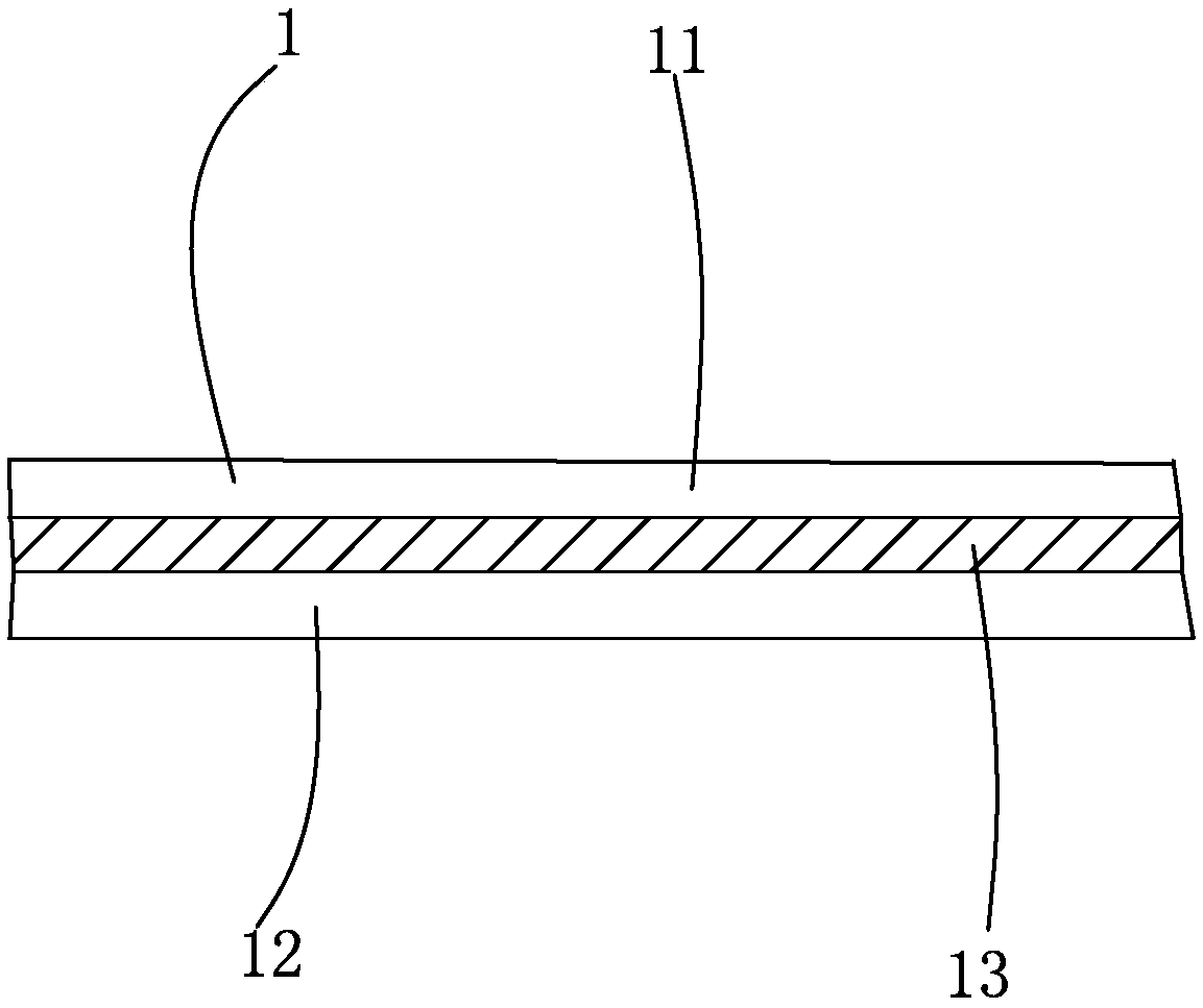
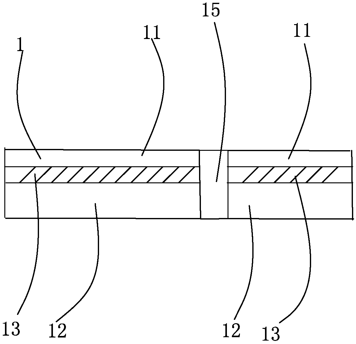
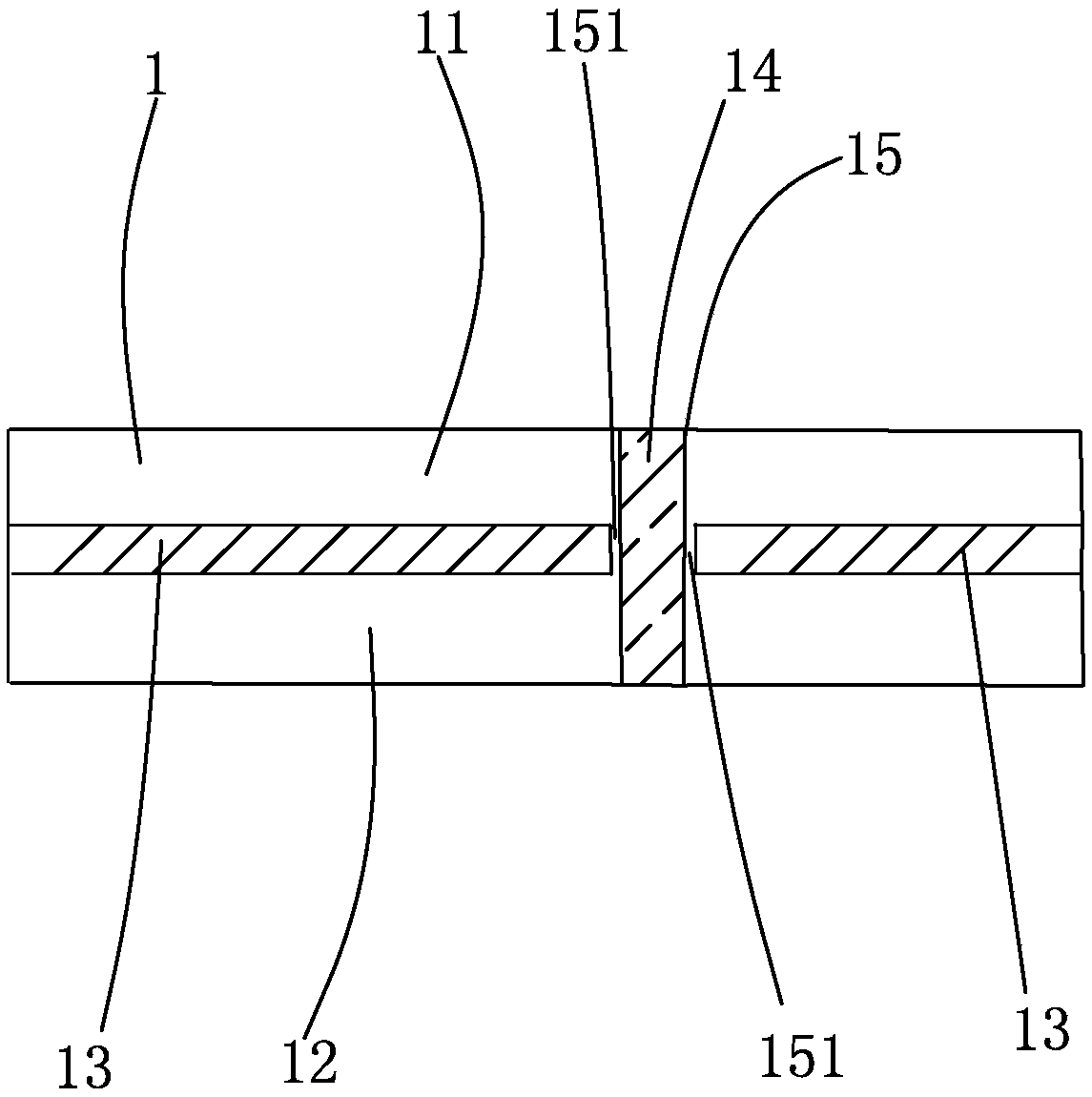
[0055] ① Select a copper-clad core board with copper foils of different thicknesses on both sides as the first copper-clad core board 1. The first copper-clad core board 1 includes a first copper foil 11 located on the first copper The core board 13 on one side of the foil 11 and the second copper foil 12 located on the other side of the core board 13, the second copper foil 12 is thickened through the plate surface electroplating process, see figure 1 Specifically, the thickness of the first copper foil 11 is 0.7mil, the thickness of the second copper foil 12 is 1.4mil, and a layer of corrosion-resistant film is made on the first layer of copper foil 11, and the second Layer copper foil...


PUM

PropertyMeasurementUnit
thicknessaaaaaaaaaa
thicknessaaaaaaaaaa
thicknessaaaaaaaaaa

Abstract

The invention discloses a blind hole circuit board and a manufacturing method thereof. The method comprises the following steps: processing copper-clad core boards, respectively processing two copper-clad core boards covered with copper foils in different thickness, drilling a through hole on a first copper-clad core board to make a blind hole, and thickening copper layer thickness of a second copper foil of the first copper-clad core board through panel plating, processing a second copper foil to a second circuit layer, thickening copper layers on two surfaces of a second copper-clad core board and manufacturing a third circuit layer, and laminating the first and second copper-clad core boards and a prepreg to an integrated circuit board; mechanically drilling a through hole on the laminated integrated circuit board and plating a layer of copper, thickening an outer layer copper foil of the integrated circuit board through panel plating, and manufacturing a circuit of an outer surfacelayer and covering a solder mask, and then perform surface treatment. The copper-clad core boards with copper foils in different thicknesses are used. In processes of plating through holes, panel plating, and pattern plating, in order to achieve thickness requirement of copper of a hole, the copper layer would not be plated too thick, and overall board thickness can be conveniently controlled.

Description

【Technical field】 [0001] The invention relates to the technical field of printed circuit boards, in particular to a blind hole circuit board and a manufacturing method thereof. 【Background technique】 [0002] In the existing printed circuit board technology, for circuit boards with mechanical blind hole design, through holes are usually drilled on the copper clad core board of the blind hole layer, and then the single plated hole process is performed, and then laminated layer by layer. combine. However, in the plating process, the plating process needs to make a plated film one more time, and then plate the hole, remove the film and grind away the copper protruding from the hole when the hole is plated. The process is cumbersome and the copper grinding of the hole is difficult to control, making the production cost higher. ; Instead of using the plating process to directly plate the entire board to make blind hole copper, affected by the electroplating principle, the copper...

Claims


Application Information

Patent Timeline
Patent Type & Authority Applications(China)
IPC IPC(8): H05K3/42H05K3/46
CPCH05K3/421H05K3/429H05K3/4623
Inventor 莫介云
Owner 广东依顿电子科技股份有限公司
Why Eureka
Try Eureka