Array substrate and manufacturing method thereof
一种阵列基板、制造方法的技术,应用在平板显示领域,能够解决抗静电能力减弱、边框设计窄、增加线宽难实现等问题,达到平衡消耗电荷量的效果
- Summary
- Abstract
- Description
- Claims
- Application Information
AI Technical Summary
Problems solved by technology
Method used
Image

Examples
Embodiment Construction
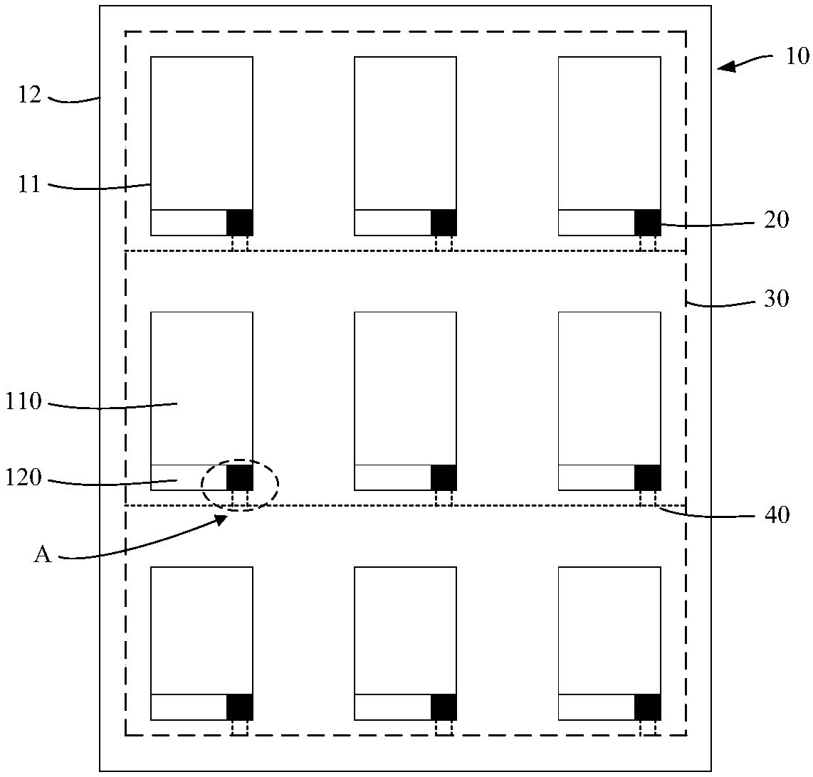
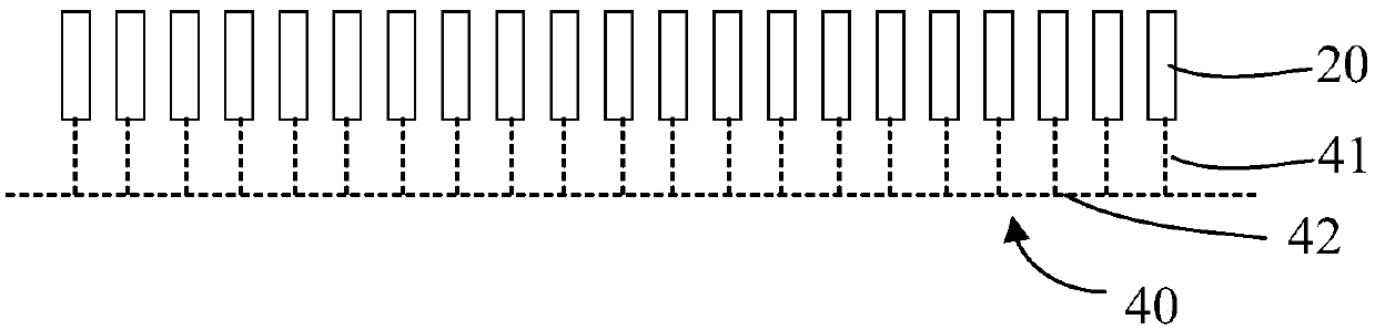
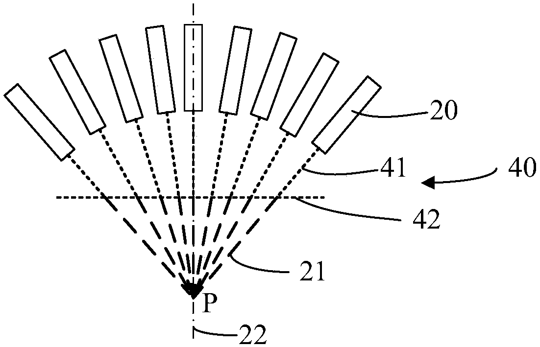
[0025] As mentioned in the background art, due to the narrow edge wiring area, the antistatic capability is weakened. During the production process, static electricity will inevitably be generated when equipment or personnel touch the product, and the generated static electricity will easily cause product damage and affect the yield rate of the product.
[0026] In order to avoid static electricity loss, the present invention provides an array substrate, comprising: a base substrate, a plurality of sets of binding terminals located on the base substrate, a first electrostatic protection line located on the edge region of the base substrate, and a second ESD protection line located on the base substrate, wherein the binding terminal is connected to the first ESD protection line through the second ESD protection line.
[0027] In the array substrate provided by the present invention, multiple groups of binding terminals are formed on the base substrate, a first static protection...
PUM
 Abstract
Description
Claims
Application Information
 - R&D
- Intellectual Property
- Life Sciences
- Materials
- Tech Scout
- Unparalleled Data Quality
- Higher Quality Content
- 60% Fewer Hallucinations
Browse by: Latest US Patents, China's latest patents, Technical Efficacy Thesaurus, Application Domain, Technology Topic, Popular Technical Reports.
© 2025 PatSnap. All rights reserved.Legal|Privacy policy|Modern Slavery Act Transparency Statement|Sitemap|About US| Contact US: help@patsnap.com