Display substrate and display device
A technology for display substrates and display devices, which is applied to semiconductor devices, electrical components, circuits, etc., can solve problems such as the reduction of screen brightness, and achieve the effect of avoiding the reduction of image brightness.
- Summary
- Abstract
- Description
- Claims
- Application Information
AI Technical Summary
Problems solved by technology
Method used
Image
Examples
no. 1 example
[0025] The invention provides a display substrate.
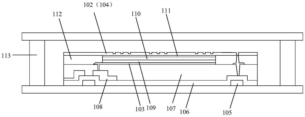
[0026] like figure 1 As shown, in one embodiment, the display substrate includes a base substrate 101 and an anti-peep layer 102 disposed on the base substrate 101 , and the base substrate 101 has a plurality of pixel regions.
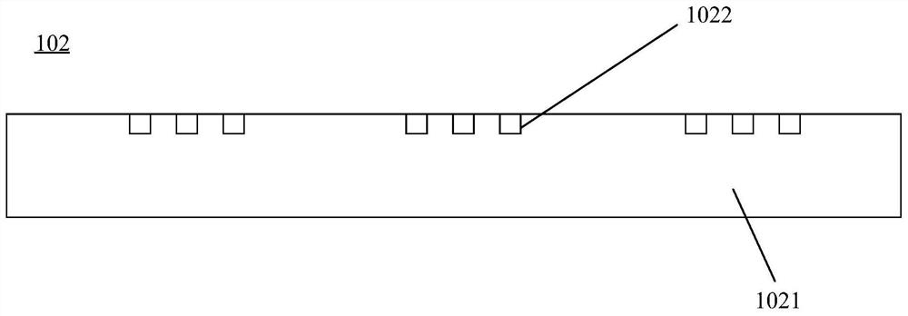
[0027] like figure 2 As shown, the anti-peeping layer 102 includes a light propagation layer 1021 and a plurality of directional gratings 1022 , and one directional grating 1022 corresponds to at least one pixel region on the base substrate 101 .
[0028] The directional grating 1022 in this embodiment is used to direct the light that enters the light propagation layer 1021 out. It can only shoot in a specific direction. In this way, only in the outgoing direction of the light, the content displayed on the screen can be observed, and in other directions, the content displayed on the screen cannot be observed, thereby achieving the effect of anti-peeping.
[0029] The anti-peeping layer 102 may c...
no. 2 example
[0060] The present invention also provides a display device, which comprises any one of the above display substrates.
[0061] Among them, the display device may include: mobile phone, tablet computer, e-book reader, MP3 player, MP4 player, digital camera, laptop computer, vehicle computer, desktop computer, set-top box, smart TV, wearable device at least one of the .
[0062] Since the technical solution of this embodiment includes all the technical solutions of the above-mentioned embodiments, at least all the above-mentioned technical effects can be achieved, and details will not be repeated here.
no. 3 example
[0064] The present invention also provides a method for preparing a display substrate, which is used for preparing any one of the display substrates in the above embodiments.
[0065] In one embodiment, the method comprises the steps of:
[0066] providing a base substrate 101, and forming an anti-peeping layer 102 on the base substrate 101;
[0067] Wherein, the base substrate 101 has a plurality of pixel regions, the anti-peeping layer 102 includes a light propagation layer 1021 and a plurality of directional gratings 1022, and the directional gratings 1022 are used to direct the light entering the light propagation layer 1021 The light is oriented and emitted, and one directional grating 1022 corresponds to at least one pixel area on the base substrate 101 .
[0068] The base substrate 101 in this embodiment may refer to the base substrate 101 in the existing display substrate, and the anti-peeping layer 102 formed may also refer to the anti-peeping layer 102 in the above-...
PUM
| Property | Measurement | Unit |
|---|---|---|
| length | aaaaa | aaaaa |
| width | aaaaa | aaaaa |
Abstract
Description
Claims
Application Information


