
Optical fingerprint imaging device and display

An imaging device and fingerprint technology, applied in optics, optical components, instruments, etc., can solve problems such as reducing fingerprint recognition rate and interference, and achieve the effect of improving fingerprint recognition accuracy and reducing interference light.

Active Publication Date: 2019-05-21
GUANGZHOU GOVISIONOX TECH CO LTD
View PDF7 Cites 9 Cited by
  • Summary
  • Abstract
  • Description
  • Claims
  • Application Information

AI Technical Summary

Problems solved by technology

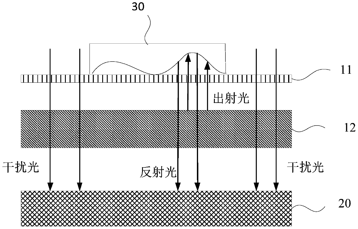
[0004] However, in practical applications, in addition to the light generated by the OLED, there are various interfering lights in the surrounding natural environment. These interfering lights will also be received by the fingerprint image sensor through the touch screen, so as to identify the skin of the finger to the fingerprint image sensor. The formed reflected light causes interference and reduces the recognition rate of fingerprints

Method used


Image

  • Optical fingerprint imaging device and display
  • Optical fingerprint imaging device and display
  • Optical fingerprint imaging device and display

Examples


Embodiment Construction

[0028] In order to make the purpose, technical solutions and advantages of the embodiments of the present invention clearer, the technical solutions in the embodiments of the present invention will be clearly and completely described below in conjunction with the drawings in the embodiments of the present invention. Obviously, the described embodiments It is a part of embodiments of the present invention, but not all embodiments.

[0029] Based on the embodiments of the present invention, all other embodiments obtained by persons of ordinary skill in the art without making creative efforts belong to the protection scope of the present invention. In the case of no conflict, the following embodiments and features in the embodiments can be combined with each other.

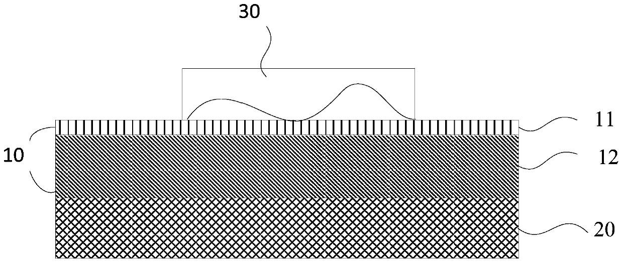
[0030] figure 1 It is a schematic structural diagram of an existing optical fingerprint imaging device, such as figure 1 As shown, it includes: a display component 10 including at least an OLED layer 12 and a cover...


PUM


Abstract

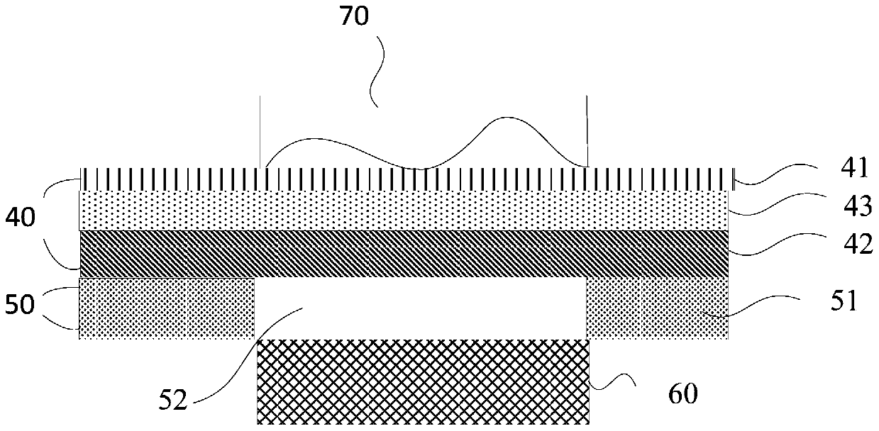
The invention provides an optical fingerprint imaging device and a display, relates to the technical field of display, and is used for solving the technical problem that natural light interferes withreflected light formed when a fingerprint image sensor identifies finger epidermis. The optical fingerprint imaging device comprises a display module, an optical conversion module and a fingerprint recognition layer which are arranged in a stacked mode. The display module comprises a cover plate and an OLED layer. Light emitted by the OLED layer is reflected by finger skin covering the surface ofthe cover plate to form reflected light containing fingerprint information. The reflected light is received by the fingerprint identification layer after passing through the display module and the optical conversion module in sequence to form a fingerprint image. The display module further comprises a first polaroid located between the cover plate and the OLED layer and a second polaroid located between the cover plate and the OLED layer. The optical conversion module comprises a second polaroid. The second polarizer is provided with a through hole area, and the through hole area corresponds to the fingerprint identification layer.

Description

technical field [0001] The invention relates to the field of display technology, in particular to an optical fingerprint imaging device and a display. Background technique [0002] Optical fingerprint imaging technology uses a fingerprint image sensor to collect reflected light on the surface of the finger skin, and then forms a fingerprint image on the surface of the finger skin based on the reflected light. With the development of terminal technology, optical fingerprint imaging technology is more and more applied in terminal devices including touch screens. [0003] In the prior art, the OLED (Organic Light-Emitting Diode, Organic Light-Emitting Diode) in the touch screen is mainly used as the light source, and the light emitted by the OLED is reflected when it reaches the finger skin on the surface of the touch screen, forming a fingerprint facing the bottom of the touch screen. Reflected light transmitted by the image sensor. The fingerprint image sensor receives the ...

Claims


Application Information

Patent Timeline
IPC IPC(8): G06K9/00G02B27/28
Inventor 李勇陈心全
Owner GUANGZHOU GOVISIONOX TECH CO LTD
Learn More