Termination structure of split gate vdmos devices

A terminal structure and separation gate technology, which is applied in semiconductor devices, electrical solid state devices, electrical components, etc., can solve the problems of affecting device withstand voltage, increasing design difficulty, and complex charge balance, etc.

Active Publication Date: 2021-04-23
UNIV OF ELECTRONICS SCI & TECH OF CHINA
View PDF6 Cites 0 Cited by
  • Summary
  • Abstract
  • Description
  • Claims
  • Application Information

AI Technical Summary

Problems solved by technology

At present, in the layout structure of conventional split-gate VDMOS devices, the split-gate deep groove is not connected to the first deep groove of the terminal, and it is necessary to separately design the lead-out of the two, as well as the spacing between the two parameters, which makes the design more difficult
Furthermore, the three-dimensional depletion effect of this region becomes significant and the charge balance becomes complicated
The above two reasons not only make this region may have premature breakdown and affect the withstand voltage of the device, but also pose new challenges to the layout design of the device

Method used


Image

  • Termination structure of split gate vdmos devices
  • Termination structure of split gate vdmos devices
  • Termination structure of split gate vdmos devices

Examples


Embodiment 1

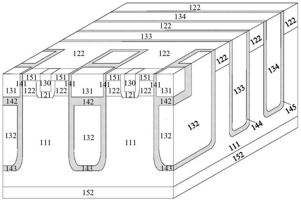
[0026] Such as image 3 and Figure 4 As shown, it is a schematic structural diagram of the split-gate VDMOS device in Example 1 of the present invention, including the structure of the active region and the structure of the terminal region:

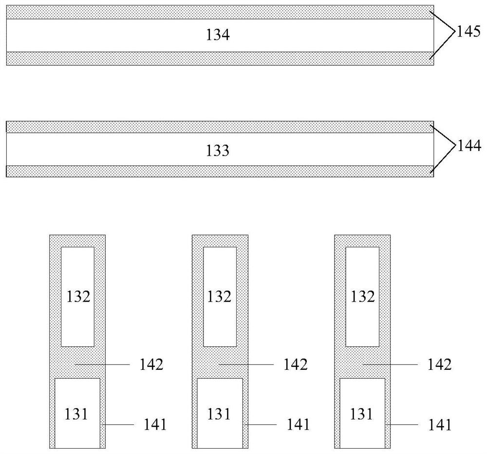
[0027] The active region structure includes: a first conductivity type substrate 152, a first conductivity type drift region 111, a first conductivity type source contact region 151, a second conductivity type well region 122, and a second conductivity type source contact region 121, the source metal contact 130, the first dielectric oxide layer 141, the second dielectric oxide layer 142, the third dielectric oxide layer 143, the control gate polysilicon electrode 131, and the separation gate polysilicon electrode 132; the drift region 111 of the first conductivity type is located in the second Above the substrate 152 of a conductivity type, the well region 122 of the second conductivity type is located above the drift region 111 of the...

Embodiment 2

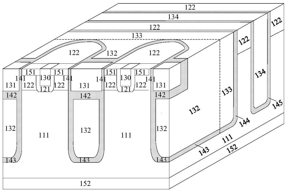
[0035] Such as Figure 5As shown, it is a schematic diagram of the terminal structure of the split-gate VDMOS device in Embodiment 2 of the present invention. The difference between this example and Embodiment 1 is that the arc diameter at the junction of the split-gate deep groove and the first terminal deep groove is larger than the separation pitch of deep trenches. The purpose is to further alleviate the curvature effect and optimize the charge balance, the principle of which is basically the same as that of Embodiment 1.

Embodiment 3

[0037] Such as Figure 6 As shown, it is a schematic diagram of the terminal structure of the split-gate VDMOS device in Embodiment 3 of the present invention. The difference between this example and Embodiment 1 is that the connection between the split-gate deep groove and the first terminal deep groove is at a right angle, and the connection is not opposite. The structure is chamfered to reduce the difficulty of design and manufacture, and the principle is basically the same as that of Embodiment 1.


PUM


Abstract

The invention provides a terminal structure of a split gate VDMOS device, including an active region structure and a termination region structure. The invention connects the split gate deep groove with the first terminal deep groove, and the two share a contact hole for leading out, reducing the The parameters to be considered when designing the device layout structure simplify the design of the device layout structure, and at the same time convert the three-dimensional depletion into two-dimensional depletion, and make a special design for the structure of the connection between the deep groove of the separation gate and the deep groove of the first terminal, Further alleviate the curvature effect, optimize the charge balance, and improve the withstand voltage of the terminal structure.

Description

technical field [0001] The invention belongs to the field of power semiconductors, and in particular relates to a terminal structure of a split-gate VDMOS device. Background technique [0002] Power semiconductor devices have been widely used in consumer electronics, computers and peripherals, network communications, electronic special equipment and instruments due to their characteristics of high input impedance, low loss, fast switching speed, no secondary breakdown, and wide safe working area. Instrumentation, automotive electronics, LED display and electronic lighting and many other aspects. Compared with conventional VDMOS devices, VDMOS devices with a split gate structure have better performance due to the introduction of the split gate. The split gate electrode introduced by the split gate VDMOS device is short-circuited to the source, which can be regarded as an internal field plate, and the electric field in the drift region is modulated by MOS depletion, so that t...

Claims


Application Information

Patent Timeline
Patent Type & Authority Patents(China)
IPC IPC(8): H01L29/78H01L29/06H01L29/423H01L27/02
CPCH01L27/0207H01L29/0615H01L29/0684H01L29/42356H01L29/7802
Inventor 章文通何俊卿王睿杨昆乔明王卓张波李肇基
Owner UNIV OF ELECTRONICS SCI & TECH OF CHINA
Why Eureka
Try Eureka