Mounting structure of electronic component

A technology of electronic components and installation structures, which is applied in the direction of electrical components, electrical equipment structural parts, electrical equipment shells/cabinets/drawers, etc., which can solve the problems of inability to realize plug-in replacement operations, more dust falling, and shortened service life and other problems, to achieve the effect of internal dust prevention and component cooling operations, simple disassembly, maintenance and replacement operations, and increased service life

Inactive Publication Date: 2020-02-07
徐州陀微传感科技有限公司
View PDF6 Cites 0 Cited by
  • Summary
  • Abstract
  • Description
  • Claims
  • Application Information

AI Technical Summary

Problems solved by technology

[0003] In the connection method of electronic components, the direct welding between the component pins and the PCB board is generally the main method. This connection method makes the components directly exposed to the outer surface, and a lot of dust will fall on the long-term use. The components are directly connected to the PCB board. Contact, the heat generated may cause damage to the components, shorten the service life, the connection is relatively fixed, and it is impossible to realize simple plug-in and replacement operations

Method used


Image

  • Mounting structure of electronic component
  • Mounting structure of electronic component
  • Mounting structure of electronic component

Examples


Embodiment Construction

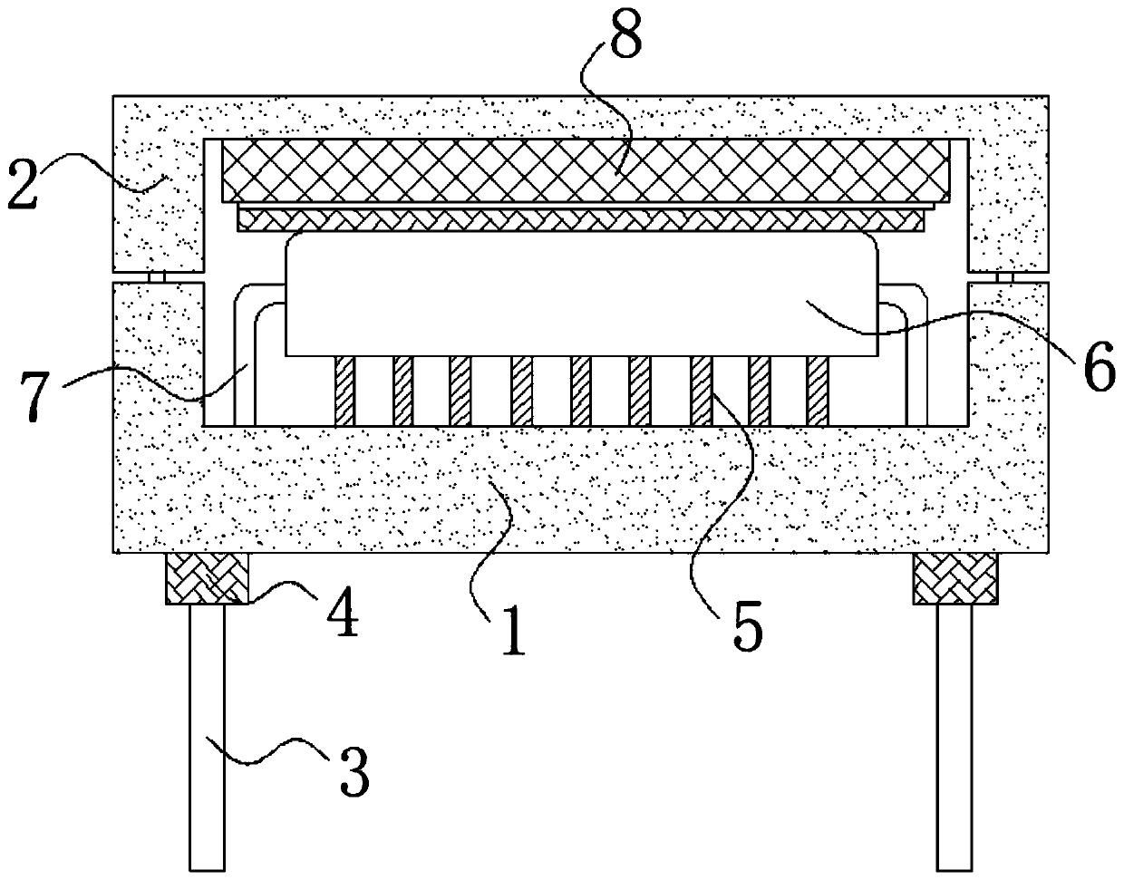
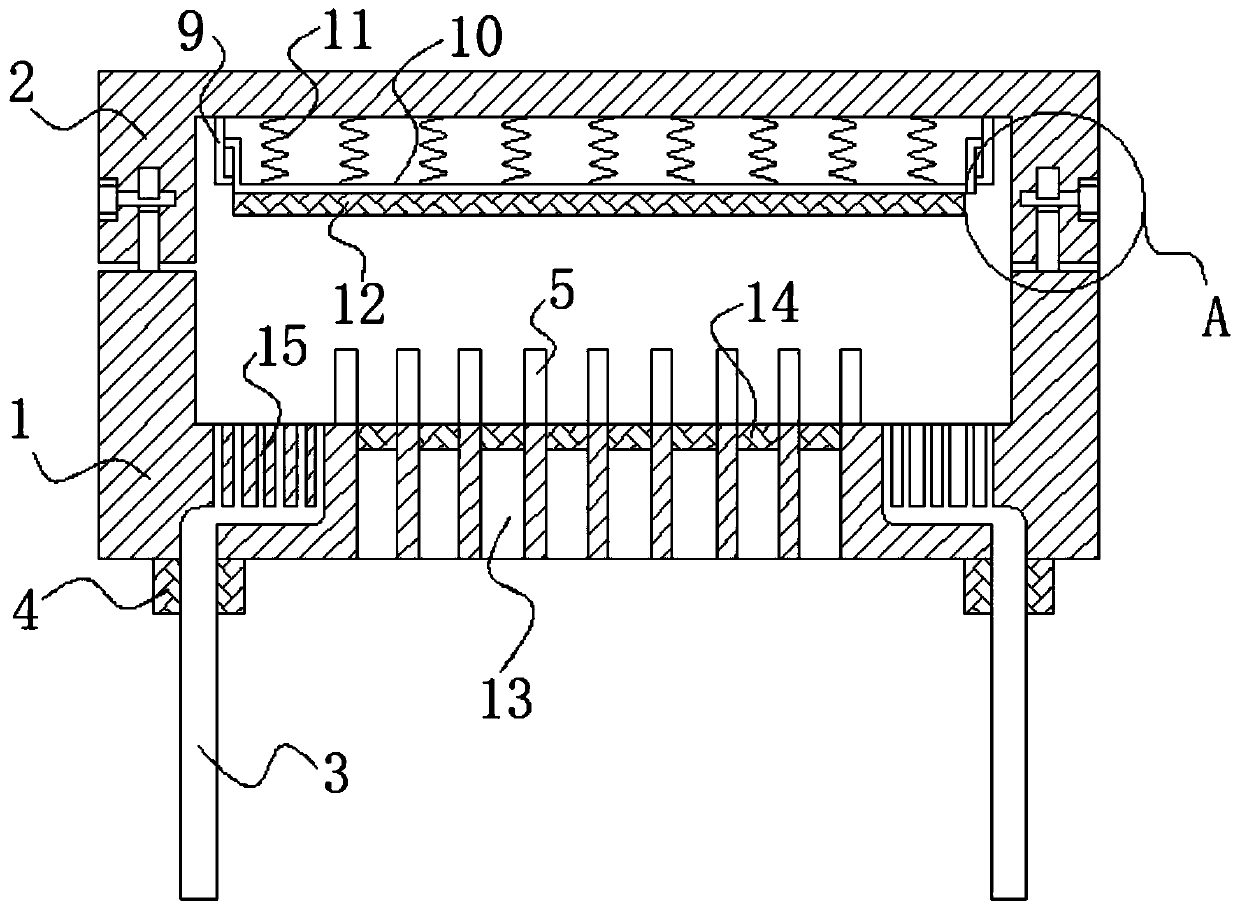
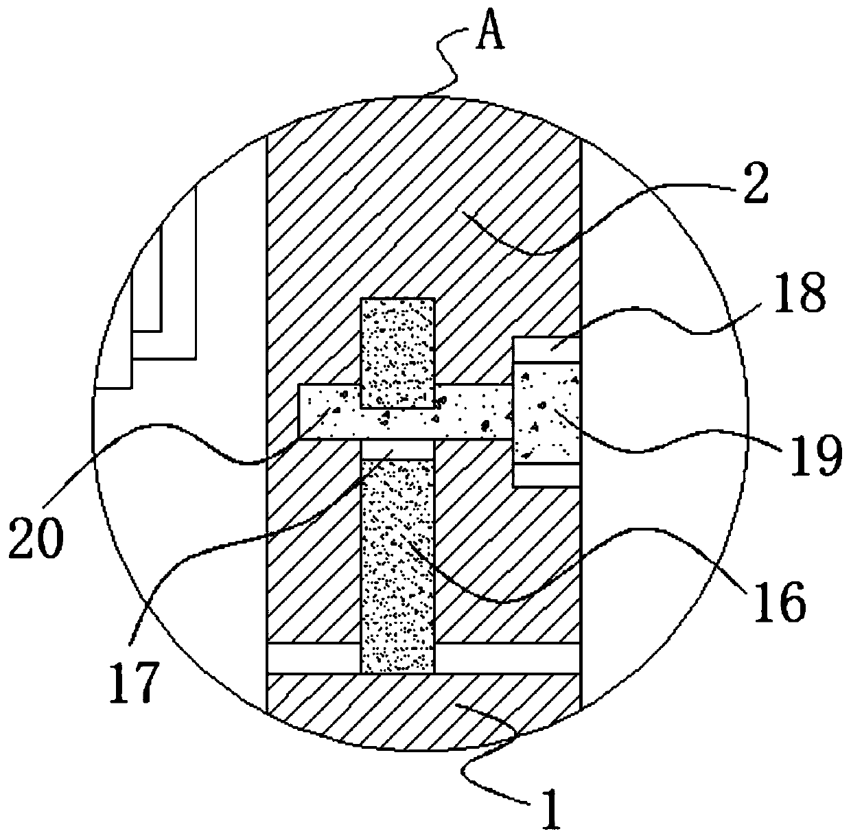
[0030] The following will clearly and completely describe the technical solutions in the embodiments of the present invention with reference to the accompanying drawings in the embodiments of the present invention. Obviously, the described embodiments are only some, not all, embodiments of the present invention. Based on the embodiments of the present invention, all other embodiments obtained by persons of ordinary skill in the art without making creative efforts belong to the protection scope of the present invention.

[0031] In the description of the present invention, it should be noted that the terms "center", "upper", "lower", "left", "right", "vertical", "horizontal", "inner", "outer" etc. The indicated orientation or positional relationship is based on the orientation or positional relationship shown in the drawings, and is only for the convenience of describing the present invention and simplifying the description, rather than indicating or implying that the referred d...


PUM


Abstract

The invention discloses a mounting structure of an electronic component. The mounting structure comprises a mounting base, connecting inserting rods are fixedly connected with the two sides of the lower surface of the mounting base respectively, and can be fixedly connected on the surface of a PCB, the upper end of the mounting base is fixedly connected with an upper cover, heat dissipation platesare fixedly arranged at the middle portion of the inner surface of the mounting base and are fixedly arranged at the upper portion of the inner surface of the mounting base at an equal intervals, andvent holes are fixedly formed in the upper surface of the mounting base and penetrate the lower surface of the mounting base. In the present invention, the mounting structure of the electronic component is directly fixed on the PCB, the electronic component is fixed in the structure to achieve fixing of the position of the electronic component, and connecting insertion holes with different distances are fixedly formed in the structure and matched with joint operation of the upper compression part, so that fixed connecting positions are provided for electronic components of different sizes; and moreover, the upper portion and the lower portion of the structure are fixedly arranged in a butt joint mode, butt joint holes are formed in the structure, the butt joint mode is simple, and simpledisassembling, maintaining and replacing operation is achieved.

Description

technical field [0001] The invention relates to the field of installation structures, in particular to an installation structure of electronic components. Background technique [0002] Electronic components are components of electronic components and small electrical machines and instruments. They are often composed of several parts and can be used in similar products; they often refer to certain parts in industries such as electrical appliances, radios, and instruments, such as capacitors and transistors. The general term for sub-devices such as hairsprings, hairsprings, etc., common ones include diodes, etc. [0003] In the connection method of electronic components, the direct welding between the component pins and the PCB board is generally the main method. This connection method makes the components directly exposed to the outer surface, and a lot of dust will fall on the long-term use. The components are directly connected to the PCB board. Contact and heat generation...

Claims


Application Information

Patent Timeline
Patent Type & Authority Applications(China)
IPC IPC(8): H05K5/00H05K5/02H05K7/20
CPCH05K5/0091H05K5/0213H05K5/0217H05K5/0247H05K7/20009H05K7/20436
Inventor 路永乐
Owner 徐州陀微传感科技有限公司
Why Eureka
Try Eureka