
Display panels and display devices

A display panel and display area technology, applied in semiconductor devices, electrical components, circuits, etc., can solve problems such as difficulty in meeting user needs, blurred optical components under the screen, etc., to improve the problem of uneven light quantity, reduce differences, and improve imaging. quality effect

Active Publication Date: 2022-07-05
XIAMEN TIANMA MICRO ELECTRONICS
View PDF8 Cites 0 Cited by
  • Summary
  • Abstract
  • Description
  • Claims
  • Application Information

AI Technical Summary

Problems solved by technology

[0004] Embodiments of the present invention provide a display panel and a display device to solve the problem in the prior art that the imaging of optical components under the screen is very blurred and difficult to meet user needs

Method used


Image

  • Display panels and display devices
  • Display panels and display devices
  • Display panels and display devices

Examples


Embodiment Construction

[0030] In order to make the purposes, technical solutions and advantages of the embodiments of the present invention clearer, the technical solutions in the embodiments of the present invention will be clearly and completely described below with reference to the accompanying drawings in the embodiments of the present invention. Obviously, the described embodiments These are some embodiments of the present invention, but not all embodiments. Based on the embodiments of the present invention, all other embodiments obtained by those of ordinary skill in the art without creative efforts shall fall within the protection scope of the present invention.

[0031] The terms used in the embodiments of the present invention are only for the purpose of describing specific embodiments, and are not intended to limit the present invention. As used in the embodiments of the present invention and the appended claims, the singular forms "a," "the," and "the" are intended to include the plural f...


PUM

PropertyMeasurementUnit
transmittivityaaaaaaaaaa

Abstract

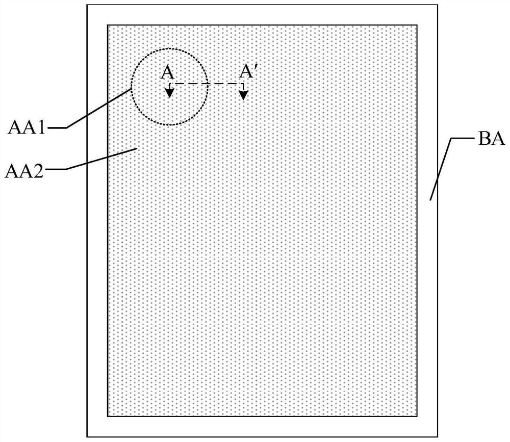
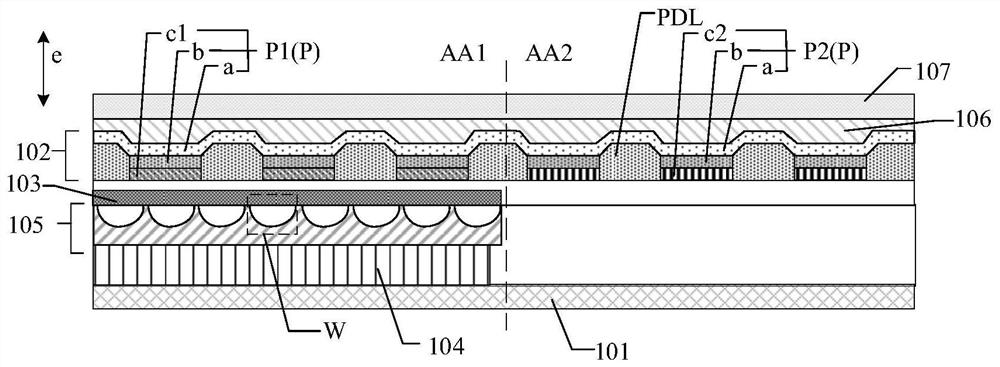
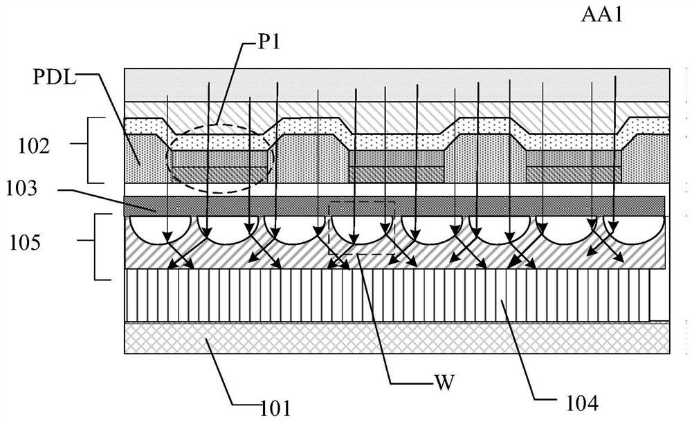
Embodiments of the present invention provide a display panel and a display device. The display area of ​​the display panel includes a first display area and a second display area; a substrate; a display layer, the display layer includes a pixel definition layer and a plurality of light-emitting devices, the first light-emitting device located in the first display area includes a first anode, and is located in the first The second light-emitting device in the two display areas includes a second anode, and the light transmittance of the first anode is greater than that of the second anode; the state switching layer is located on the side of the display layer away from the display surface of the display panel, and the state switching layer is connected to the first anode. The light-emitting devices are overlapped, and the light transmittance of the state switching layer in the first state is smaller than that in the second state; the optical element is located on the side of the state switching layer away from the display layer; the uniform light structure layer is located on the state switching layer and Between the optical elements, it is used for diffusing the light emitted by the state switching layer. The invention can increase the amount of light received by the optical element, improve the unevenness of the light amount after the light penetrates the first display area, and improve the imaging quality.

Description

technical field [0001] The present invention relates to the field of display technology, and in particular, to a display panel and a display device. Background technique [0002] With the development of display technology, people not only require a smooth user experience for the electronic products they use, but also have higher and higher requirements for visual experience. High screen ratio has become the current research direction. For electronic products, the setting of optical components such as the front camera will inevitably occupy a certain space, thus affecting the screen ratio. In order to achieve a true full screen, the researchers considered the realization of optical components under the screen. [0003] The optical element such as a camera is arranged below the light-emitting device of the display panel, that is, the optical element is arranged in the display area, and the position of the optical element can be displayed normally. When the optical element is ...

Claims


Application Information

Patent Timeline
Patent Type & Authority Patents(China)
IPC IPC(8): H01L27/32H01L51/50H01L51/52
CPCH10K59/122H10K50/00H10K50/81H10K50/854
Inventor 刘育豪牛晶华戴铭志
Owner XIAMEN TIANMA MICRO ELECTRONICS
Learn More