Pixel driving circuit and driving method thereof, display panel and display equipment

A technology of pixel driving circuit and pixel unit, which is applied in static indicators, instruments, etc., can solve the problems of inability to meet, cannot achieve a narrower border or even no border, and achieve the effect of borderless.

Active Publication Date: 2020-07-14
HEFEI BOE DISPLAY TECH CO LTD +1
View PDF10 Cites 0 Cited by
  • Summary
  • Abstract
  • Description
  • Claims
  • Application Information

AI Technical Summary

Problems solved by technology

[0003] However, since the GOA circuit is set on both sides of the OLED display panel, the frame of the OLED display panel must be set with a certain width, which directly restricts the current OLED display panel from being able to achieve a narrower frame or even a frameless design. Therefore, It cannot meet the current demand for narrower borders or even borderless OLED products, and needs to be resolved urgently

Method used


Image

  • Pixel driving circuit and driving method thereof, display panel and display equipment
  • Pixel driving circuit and driving method thereof, display panel and display equipment
  • Pixel driving circuit and driving method thereof, display panel and display equipment

Examples


Embodiment Construction

[0025] Embodiments of the present invention are described in detail below, examples of which are shown in the drawings, wherein the same or similar reference numerals designate the same or similar elements or elements having the same or similar functions throughout. The embodiments described below by referring to the figures are exemplary and are intended to explain the present invention and should not be construed as limiting the present invention.

[0026] A pixel driving circuit according to an embodiment of the present invention will be described below with reference to the accompanying drawings.

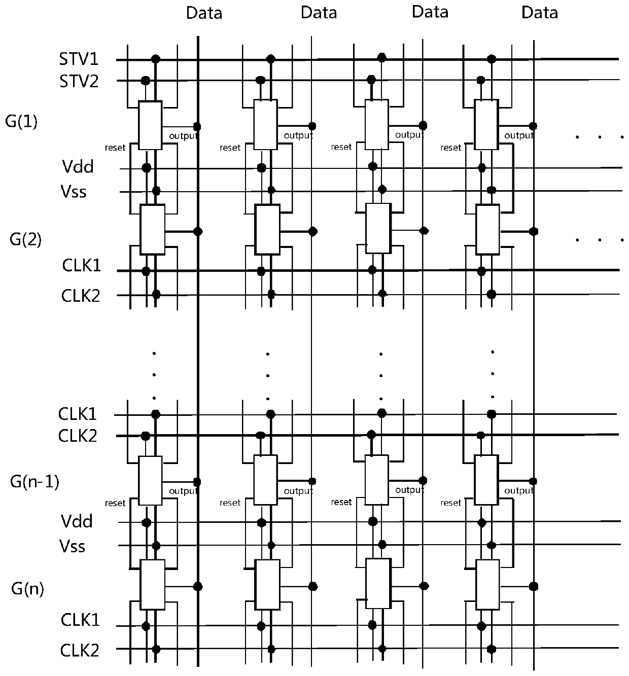
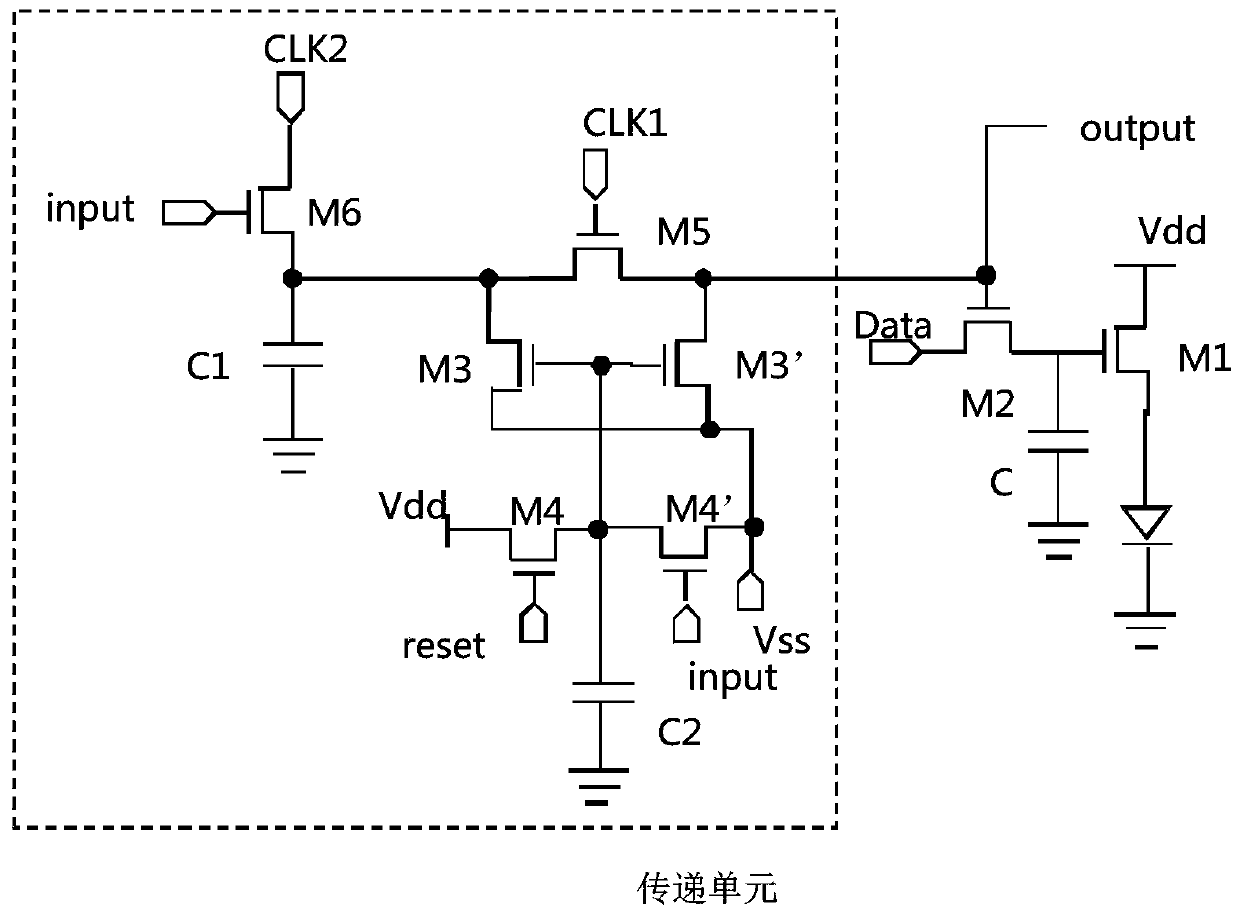
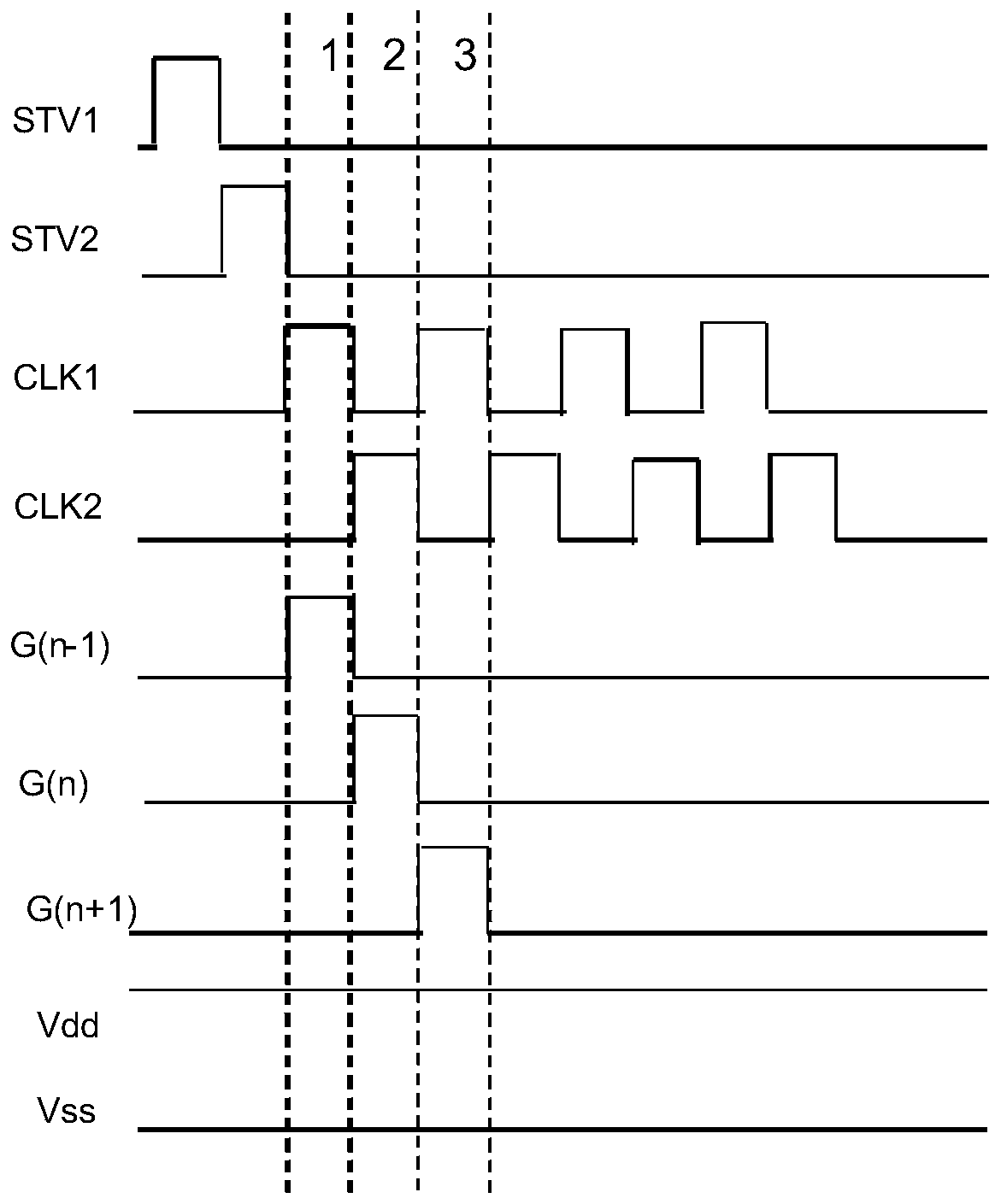
[0027] figure 1 It is a schematic structural diagram of a pixel driving circuit provided by an embodiment of the present invention.

[0028] As analyzed in the background technology, in the related art, because the GOA circuit is arranged on both sides of the OLED display panel, the frame of the OLED display panel must be set with a certain width, which directly restricts the c...


PUM


Abstract

The invention provides a pixel driving circuit and a driving method thereof, a display panel and display equipment. The pixel driving circuit comprises a plurality of rows and columns of pixel units;in each column of pixel units, when a first clock in a current row of pixel units is at a high potential and a second clock is at a low potential, a first capacitor is controlled to be charged according to a high potential signal output by the output end of a previous row of pixel units; when the first clock is at a low potential and the second clock is at a high potential, the stored high potential signal is output to the output end by the first capacitor, so as to control the light emitting layer to emit light according to the stored high potential signal by the first capacitor; resetting operation is performed according to the high potential signal output by the output end of the pixel unit in the next row, and the output end of the pixel unit in the current row is set as a low potential so as to realize line-by-line driving of the pixel units in the same column. The technical problem that in the prior art, the design of a narrow frame or even no frame cannot be realized via a conventional OLED display panel is solved.

Description

technical field [0001] The present invention relates to the field of display technology, in particular to a pixel driving circuit and a driving method thereof, a display panel and a display device. Background technique [0002] Array substrate row drive (GOA) technology is to use the existing liquid crystal display panel array (Array) process to fabricate the gate row scanning drive signal circuit on the array substrate to realize the driving method of progressive scanning of the gate. Because the row driving technology of the array substrate can save the gate driver IC (gate IC) and reduce the width of the frame to a certain extent, it has been widely used in the design of organic light emitting diode (OLED) display panels. [0003] However, since the GOA circuit is set on both sides of the OLED display panel, the frame of the OLED display panel must be set with a certain width, which directly restricts the current OLED display panel from being able to achieve a narrower fr...

Claims


Application Information

Patent Timeline
Patent Type & Authority Applications(China)
IPC IPC(8): G09G3/3266
CPCG09G3/3266
Inventor 陈凯刘冬韩飞吴旺娣李方庆陈沫
Owner HEFEI BOE DISPLAY TECH CO LTD
Why Eureka
Try Eureka