
An organic photodetector based on optical microcavity effect and its preparation method

A photodetector, optical microcavity technology, applied in photovoltaic power generation, electric solid state device, semiconductor/solid state device manufacturing, etc. Good detection ability, unique structure effect

Active Publication Date: 2022-08-02
UNIV OF ELECTRONICS SCI & TECH OF CHINA
View PDF4 Cites 0 Cited by
  • Summary
  • Abstract
  • Description
  • Claims
  • Application Information

AI Technical Summary

Problems solved by technology

[0003] Traditional organic photodetectors have low external quantum efficiency in the near-infrared band due to the difficulty in separating long-wavelength excitons, which in turn leads to low detectivity.

Method used


Image

  • An organic photodetector based on optical microcavity effect and its preparation method
  • An organic photodetector based on optical microcavity effect and its preparation method

Examples


Embodiment 1

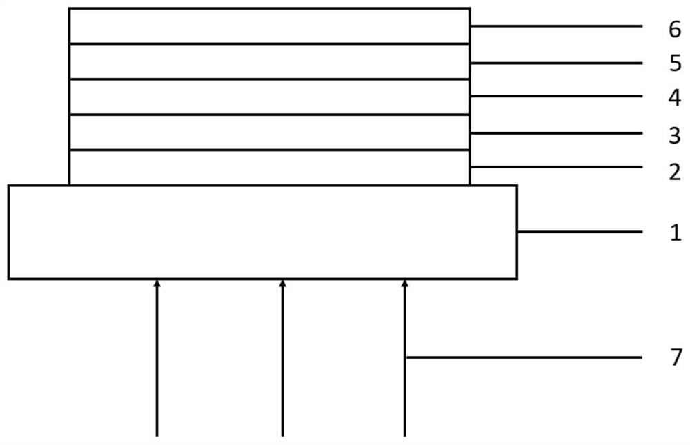
[0035] Cleaning the glass substrate 1: put the glass substrate 1 into detergent, acetone, deionized water, and isopropanol in sequence, ultrasonically clean for 15 minutes each time, and then blow dry with an inert gas. Then transfer the glass substrate 1 to the vacuum evaporation equipment, and the vacuum degree is less than 3.0×10 -3 A layer of Au electrode was evaporated in a Pa environment. Then, the transparent conductive electrode layer 2 was put into an ozone machine for UV treatment for 10 min. The mixture of PEIE and benzothiazole cyanine dye was spin-coated on the transparent conductive electrode layer 2 after ozone treatment, and the rotational speed was controlled to be 4000 rpm and the time was 20 s. . The glass substrate 1 and the organic donor-acceptor solution that have been spin-coated with the double-narrowband modulation layer 3 were preheated at 100 °C, and the acceptor solution was spin-coated on the surface of the double-narrowband modulation layer 3 wi...

Embodiment 2

[0038] Cleaning the glass substrate 1: put the glass substrate 1 into detergent, acetone, deionized water, and isopropanol in sequence, ultrasonically clean for 15 minutes each time, and then blow dry with an inert gas. Then transfer the glass substrate 1 to the vacuum evaporation equipment, and the vacuum degree is less than 3.0×10 -3 A layer of Au electrode was evaporated in a Pa environment. Then, the transparent conductive electrode layer 2 was put into an ozone machine for UV treatment for 10 min. The mixture of PEIE and benzothiazole cyanine dye was spin-coated on the transparent conductive electrode layer 2 after ozone treatment, and the rotational speed was controlled to be 4000 rpm and the time was 20 s. . The glass substrate 1 and the organic donor-acceptor solution that have been spin-coated with the double-narrowband modulation layer 3 were preheated at 100 °C, and the acceptor solution was spin-coated on the surface of the double-narrowband modulation layer 3 wi...


PUM

PropertyMeasurementUnit
thicknessaaaaaaaaaa
thicknessaaaaaaaaaa
thicknessaaaaaaaaaa

Abstract

The invention discloses an organic photoelectric detector based on an optical microcavity effect and a preparation method thereof, belonging to the field of photoelectric detection devices. The photodetectors are sequentially arranged from bottom to top as follows: a glass substrate, a semi-transparent conductive electrode layer, a double narrow-band modulation layer, an organic functional layer, a hole transport layer, and a metal electrode layer. The optical microcavity structure composed of the semi-transparent conductive electrode layer, the double narrowband modulation layer, the organic functional layer, the hole transport layer and the metal electrode layer can realize the double narrowband response to different wavelength bands, so as to have the dual band narrowband detection capability. . The invention effectively solves the problems that the organic photoelectric detector has a large half-wave peak width, poor detection performance in the near-infrared band and only has a single-band detection capability.

Description

technical field [0001] The invention relates to the technical field of photodetection devices, in particular to an organic photodetector based on an optical microcavity effect and a preparation method thereof. Background technique [0002] Compared with inorganic photovoltaic devices, organic photovoltaic devices have the characteristics of simple production process, low cost, and can be fabricated on different substrates in a large area. Coupled with the rapid development of organic photovoltaic devices, they have been widely used in organic solar cells and organic light detection. equipment and other fields. Organic photodetectors have the characteristics of easy integration and are widely used in many consumer electronic products, health care, resource detection, environmental protection and so on. In order to meet the requirements of practical applications, organic photodetectors should have high detection rate and narrow spectral response range to achieve more accurate...

Claims


Application Information

Patent Timeline
Patent Type & Authority Patents(China)
IPC IPC(8): H01L51/46H01L51/44H01L51/48H01L51/42
CPCH10K71/12H10K71/40H10K85/611H10K85/657H10K30/80H10K30/30Y02E10/549
Inventor 钟建刘洁尘李娜刘泽宇贾晓伟
Owner UNIV OF ELECTRONICS SCI & TECH OF CHINA
Features
  • Generate Ideas
  • Intellectual Property
  • Life Sciences
  • Materials
  • Tech Scout
  • Unparalleled Data Quality
  • Higher Quality Content
  • 60% Fewer Hallucinations
Learn More