Bifunctional detector based on charge narrowing collection effect and preparation method thereof
A dual-function, detector technology, applied in the field of photoelectric detection, can solve the problem of wide half-wave peak width of perovskite photodetector, and achieve the effect of good detection ability and unique structure
- Summary
- Abstract
- Description
- Claims
- Application Information
AI Technical Summary
Problems solved by technology
Method used
Image

Examples
Embodiment 1
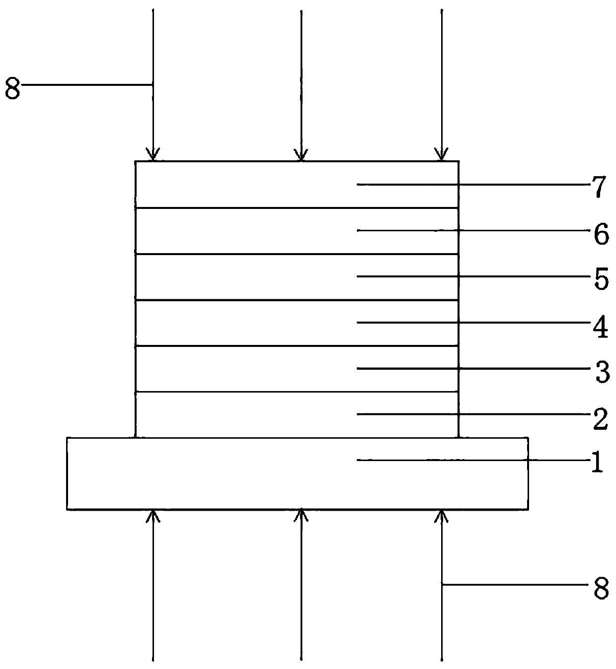
[0034] A dual-function detector based on the charge narrowing collection effect, including a glass substrate 1 coated with a transparent conductive electrode layer 2, and the transparent conductive electrode layer 2 is sequentially spin-coated with hole transport from bottom to top layer 3, a perovskite active layer 4, and an electron transport layer 5, the electron transport layer 5 is plated with a hole blocking layer 6 and a metal electrode layer 7 sequentially from bottom to top.
[0035] Wherein, the transparent conductive electrode layer 2 adopts an ITO transparent conductive electrode with a thickness of 150 nm.
[0036] The hole transport layer 3 is a PEDOT:PSS thin film with a thickness of 90 nm.
[0037] The perovskite active layer 4 adopts CH with a thickness of 1000nm 3 NH 3 PbBr 1.5 I 1.5 .
[0038] Electron transport layer 5 adopts PC with a thickness of 100nm 61 BM.
[0039] Hole blocking layer 6 adopts the C that thickness is 60nm 60 film.
[0040] The...
Embodiment 2
[0053] On the basis of Example 1, the difference between this example and Example 1 is that the perovskite active layer 4 is replaced by CH 3 NH 3 PB 2 Br 1 .
[0054] Methylamine lead iodide and methylamine lead bromide were dissolved in DMF (N-N dimethylformamide) solution at a molar ratio of 2:1, and doped with 7% mass ratio of RhodamineB, stirred at 100°C for 6h, respectively Three different ratios of perovskite precursor solutions doped with RhodamineB were obtained: CH 3 NH 3 PB 2 Br 1 .
[0055] Under standard test conditions, the light beam is drawn from the light source, and the incident light is vertically incident on the perovskite photodetector. The test result shows that the perovskite photodetector has a narrow-band detection capability at 650nm, and the half-wave peak width is 35nm. 5.6-10 12 Jones; the light beam is drawn from the light source, and the incident light 8 is vertically incident on the perovskite photodetector. The test result shows that t...
Embodiment 3
[0057] On the basis of Example 1, the difference between this example and Example 1 is that the perovskite active layer 4 is replaced by CH 3 NH 3 PB 1.5 Br 1.5 .
[0058] Methylamine lead iodide and methylamine lead bromide were dissolved in DMF (N-N dimethylformamide) solution at a molar ratio of 1:1, and mixed with 7% mass ratio of RhodamineB, stirred at 100°C for 6h, respectively Three different ratios of perovskite precursor solutions doped with RhodamineB were obtained: CH 3 NH 3 PB 2 Br 1 .
[0059] Under standard test conditions, the light beam is extracted from the light source, and the incident light 8 is vertically incident on the perovskite photodetector. The test result shows that the perovskite photodetector has a narrow-band detection capability at 620nm, and the half-wave peak width is 30nm. The rate is 5.6-10 12 Jones; the light beam is drawn from the light source, and the incident light 8 is vertically incident on the perovskite photodetector. The te...
PUM
 Abstract
Description
Claims
Application Information
 - Generate Ideas
- Intellectual Property
- Life Sciences
- Materials
- Tech Scout
- Unparalleled Data Quality
- Higher Quality Content
- 60% Fewer Hallucinations
Browse by: Latest US Patents, China's latest patents, Technical Efficacy Thesaurus, Application Domain, Technology Topic, Popular Technical Reports.
© 2025 PatSnap. All rights reserved.Legal|Privacy policy|Modern Slavery Act Transparency Statement|Sitemap|About US| Contact US: help@patsnap.com