OLED display device, power-on transmission method for compensation data and image display method

A technology for compensating data and display devices, which is applied in the field of OLED display devices and image display, and can solve problems such as charging methods that cannot meet people's needs, and achieve good image display effects, good user experience, and good compensation effects

Active Publication Date: 2020-11-06
WUHAN TIANMA MICRO ELECTRONICS CO LTD
View PDF9 Cites 4 Cited by
  • Summary
  • Abstract
  • Description
  • Claims
  • Application Information

AI Technical Summary

Problems solved by technology

[0005] In view of this, the present invention provides an OLED display device, a compensation data power-on transmission method, and an image display method to solve the problem that the charging methods limited by charging facilities such as charging piles or charging sockets in the prior art cannot meet people's needs.

Method used


Image

  • OLED display device, power-on transmission method for compensation data and image display method
  • OLED display device, power-on transmission method for compensation data and image display method
  • OLED display device, power-on transmission method for compensation data and image display method

Examples


Embodiment Construction

[0038] As mentioned in the background technology section, in the prior art, after the OLED display panel is manufactured to form an electronic client, the image compensation effect is not good in the actual use process.

[0039] The inventors have found that the problem of the above phenomenon is:

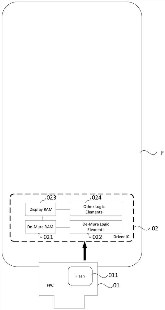
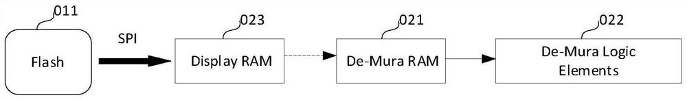
[0040] Such as figure 1 As shown, it is a schematic diagram of the compensation structure of the OLED display device in the prior art; it includes Flash011 located on the main FPC (flexible circuit board) 01 of the electronic client P for storing compensation data; the display located outside the electronic client P The display compensation value random access memory (De-Mura RAM) 021 in the driver chip (Driver IC) 02, the corresponding display compensation value logic unit (De-Mura Logic Elements) 022, and the display image data random access memory (Display RAM) 023 and Other Logic Elements (Other Logic Elements) 024. Such as figure 2 Shown is the data flow diagram of the OLE...


PUM


Abstract

The invention provides an OLED display device, a power-on transmission method for compensation data and an image display method. A display compensation value random access memory and a display compensation logic unit in a driving chip are arranged at an electronic client; the electronic client is electrically connected with the display compensation value random access memory, so that all structures communicate with one another. In the power-on non-display stage, compensation data is stored in the display compensation value random access memory of the electronic client and images are compensated through the display compensation logic unit of the electronic client. As the display compensation value random access memory and the display compensation logic unit are arranged at the electronic client, the area of the driving chip is not occupied, the area of the driving chip does not need to be increased, and the problem of distortion does not exist; different frame frequencies do not need tobe switched by erasing original data, black screen time does not exist, the image display effect is better, and the user experience is good; compensation data corresponding to different frame frequencies are directly called, so that the compensation accuracy can be ensured, and the compensation effect is better.

Description

technical field [0001] The invention relates to the field of display technology, in particular to an OLED display device, a compensation data power-on transmission method, and an image display method. Background technique [0002] At present, Active Matrix Driving OLED (AMOLED for short) has the advantages of self-illumination, high display contrast, thin thickness, wide viewing angle, fast response speed, wide operating temperature range, simple structure and manufacturing process, etc. properties are widely used. However, the current of the organic light-emitting diode will vary with the shift of the threshold voltage of the driving transistor, so that the AMOLED display panel will have non-uniform display brightness Mura (color spot defect). The Mura phenomenon means that the actual brightness of some pixels is darker or brighter than the theoretical brightness that should be displayed, which in turn affects the brightness uniformity and brightness constancy of the AMOED...

Claims


Application Information

Patent Timeline
Patent Type & Authority Applications(China)
IPC IPC(8): G09G3/3233
CPCG09G3/3233G09G2320/0233
Inventor 黑亚君王广周井雄周瑞渊
Owner WUHAN TIANMA MICRO ELECTRONICS CO LTD
Why Eureka
Try Eureka