

Multi-line array image sensor and image processing method
An image sensor and multi-line array technology, applied in the field of sensors, can solve problems such as poor flexibility
- Summary
- Abstract
- Description
- Claims
- Application Information
AI Technical Summary
Problems solved by technology
Method used
Image

Examples
Embodiment Construction
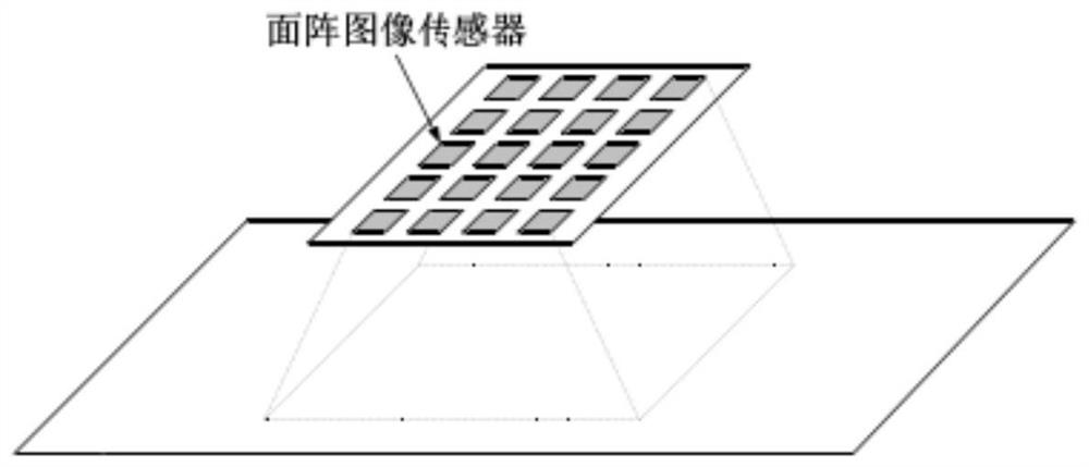
[0026] like figure 1 As shown, in the area array image sensor, the pixels are arranged in a two-dimensional area array. The area array image sensor can obtain a complete image for each exposure, so it can easily obtain two-dimensional image information. Limit its frame rate and resolution.
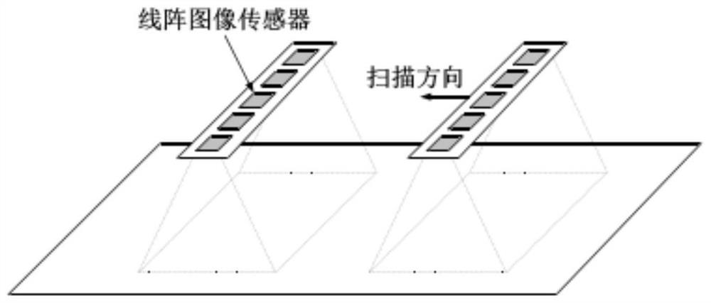
[0027] like figure 2 As shown, in the line array image sensor, the pixels are arranged in a line array form, and during the exposure period of the line array image sensor, the sensor is always moving relative to the object to be photographed. One line of image information is obtained for each exposure, and the results of multiple lines of scanning exposure are stitched to obtain complete two-dimensional image information. Although the line array image sensor cannot directly output a two-dimensional image, it contains a small number of pixels, so a large number of pixels in a line can be made, and a very high resolution can be achieved.
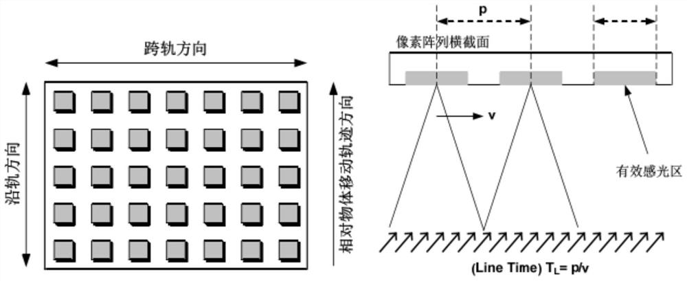
[0028] To obtain different colors or for other ...
PUM
 Abstract
Description
Claims
Application Information