
Polarization-insensitive directional coupler structure and method

A directional coupler and polarization-insensitive technology, applied in the coupling of optical waveguides, instruments, light guides, etc., can solve the problems of polarization insensitivity, birefringence, etc., and achieve easy implementation, less stringent process requirements, and broadband transmission characteristics Effect

Active Publication Date: 2021-07-30
QXP TECH INC
View PDF8 Cites 0 Cited by
  • Summary
  • Abstract
  • Description
  • Claims
  • Application Information

AI Technical Summary

Problems solved by technology

However, the SOI-based directional coupler structure also has the problem of birefringenc

Method used


Image

  • Polarization-insensitive directional coupler structure and method
  • Polarization-insensitive directional coupler structure and method
  • Polarization-insensitive directional coupler structure and method

Examples


Example Embodiment

[0050] Example 1

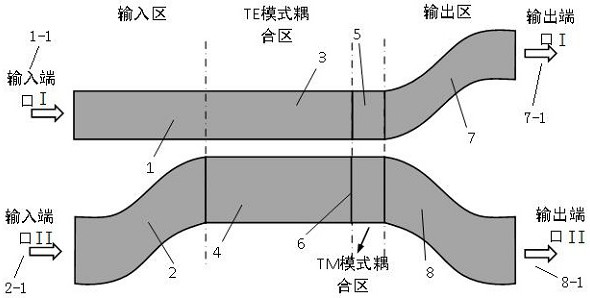
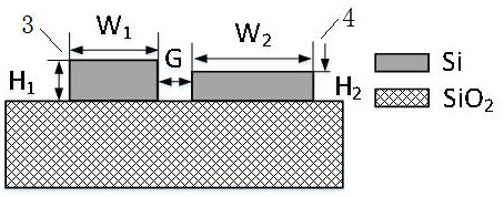
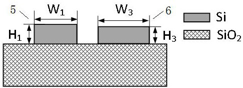
[0051] The structure of a polarization-insensitive directional coupler is as follows figure 1 shown. The cross-sectional structure of the waveguide structure in the TE mode coupling region and the TM mode coupling region is as follows: figure 2 and image 3 shown. Both the TE mode coupling region and the TM mode coupling region are asymmetric directional coupler structures. The width and height of the coupling waveguide I3 in the TE mode coupling region are W1=400nm, H1=220nm, the width and height of the coupling waveguide II4 are W2=575nm, H2=159.3nm, and the coupling spacing G=200nm. The width and height of the coupling waveguide III 5 in the TM mode coupling region are W1=400nm, H1=220nm, the height of the coupling waveguide IV 6 is H3=202.5nm, the width W3=575nm, and the coupling spacing G=200nm. The length of the curved waveguide in the output region along the beam propagation direction is 30 μm.

[0052] First, we use the beam propagation method...


PUM


Abstract

The invention provides a polarization-insensitive directional coupler structure and a method. The polarization-insensitive directional coupler structure comprises an input region, a TE mode coupling region, a TM mode coupling region and an output region. By designing a coupling waveguide structure composed of the TE mode coupling region and the TM mode coupling region, TE modes can be mutually coupled in the TE mode coupling region and are not coupled in the TM mode coupling region, and TM modes can be mutually coupled in the TM mode coupling region and are not coupled in the TE mode coupling region, so that the same splitting ratio output of the TE modes and the TM modes can be realized by optimizing the coupling waveguide structure and the coupling length, and the polarization-insensitive transmission characteristic is further realized. The directional coupler structure can also realize broadband transmission characteristics, and has important research and application values in the silicon-based photon integration field and the optical communication field.

Description

technical field [0001] The invention relates to the technical field of optical devices, in particular to a polarization-insensitive directional coupler structure and method. Background technique [0002] In recent years, the development of silicon-on-insulator (SOI) material is very rapid, because it can realize very small waveguide size, and its manufacturing process is compatible with CMOS, it is considered to be the most potential and hopeful material for realizing monolithic optoelectronic integrated circuit . However, the large refractive index difference between silicon (Si) and silicon dioxide (SiO2) makes the SOI waveguide have a strong birefringence effect, resulting in a relatively large gap between the transverse electric field mode (TE) and transverse magnetic field mode (TM). A large phase difference degrades the performance of optical devices. In order to solve this problem, devices such as polarization beam splitting and polarization conversion have been dev...

Claims


Application Information

Patent Timeline
IPC IPC(8): G02B6/27
CPCG02B6/2793
Inventor 郭菲程东
Owner QXP TECH INC
Learn More