
Control circuit of embedded optical fingerprint identification display device and embedded optical fingerprint identification display equipment

A fingerprint identification and display device technology, applied in the field of fingerprint identification, can solve the problems of increasing the difficulty of assembly, increasing processing procedures, and increasing costs, achieving the effects of reducing yield and cost, simplifying material control, and increasing water resistance

Pending Publication Date: 2022-03-15
FOCALTECH ELECTRONICS LTD
View PDF0 Cites 0 Cited by
  • Summary
  • Abstract
  • Description
  • Claims
  • Application Information

AI Technical Summary

Problems solved by technology

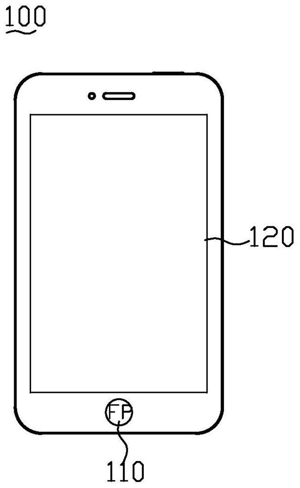
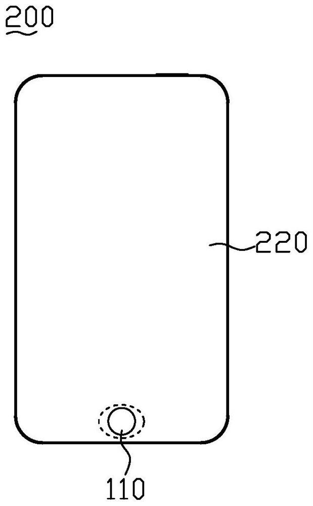
However, when cutting the display screen 220 in a different shape, it is necessary to cut the related components of the display screen (such as substrate, light guide plate, thin film transistor layer, ..., protective glass, etc.), which increases many processing procedures and increases the difficulty of assembly. degree, which increases the cost significantly

Method used


Image

  • Control circuit of embedded optical fingerprint identification display device and embedded optical fingerprint identification display equipment
  • Control circuit of embedded optical fingerprint identification display device and embedded optical fingerprint identification display equipment
  • Control circuit of embedded optical fingerprint identification display device and embedded optical fingerprint identification display equipment

Examples


Embodiment Construction

[0107] In order to make the object, technical solution and advantages of the present invention clearer, the present invention will be further described in detail below in conjunction with the accompanying drawings and embodiments. It should be understood that the specific embodiments described here are only used to explain the present invention, not to limit the present invention.

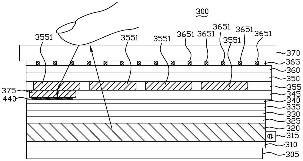
[0108] image 3 is a schematic cross-sectional view of the embedded optical fingerprint recognition display device 300 of the present invention. The embedded optical fingerprint recognition display device 300 includes a support layer (Bezel) 305, a reflector (Reflector) 310, at least one light source 315, a light guide plate (Light Guide Plate) 320, a diffuser plate (Diffuser) 325, A rear brightness enhancement film (Rear Brightenhancement Film, RBEF) 330, a front brightness enhancement film (Front Brightenhancement Film, FBEF) 335, a lower polarizer layer 340, a thin film transistor layer 345, a ...


PUM


Abstract

The invention provides a control circuit of an embedded optical fingerprint recognition display device and embedded optical fingerprint recognition display equipment, and the control circuit of the embedded optical fingerprint recognition display device comprises a multi-task unit which is provided with a plurality of multiplexers, each multiplexer is provided with a first end, a second end and a third end, the first end is connected to a corresponding data line in the plurality of data lines; the display driving unit is connected to the data line which is not connected with the plurality of multiplexers in the plurality of data lines and the second end of each multiplexer; the optical fingerprint driving and sensing unit is connected to the third end of each multiplexer; and the control unit is connected to the multitasking unit, so that the first end of each multitasking device is connected with the second end and a display operation is provided through the plurality of data lines, or the first end of each multitasking device is connected with the third end to provide a fingerprint identification operation.

Description

[0001] This application is a divisional application of a patent application with an application date of July 31, 2017, an application number of CN201710636966.8, and an invention titled "Embedded Optical Fingerprint Identification Display Device". technical field [0002] The invention relates to the technical field of fingerprint identification, in particular to an embedded optical fingerprint identification display device. Background technique [0003] Competition in the mobile phone market is becoming increasingly fierce. Therefore, many functions have been added into the mobile phone design, such as touch detection, fingerprint recognition and other functions. At the same time, in order to reduce the thickness of the mobile phone and reduce the assembly process, the current mobile phone mainly uses in-cell touch detection technology. figure 1 It is a schematic diagram of an existing mobile phone 100 . As shown in the figure, it has a fingerprint identification module 1...

Claims


Application Information

Patent Timeline
Patent Type & Authority Applications(China)
IPC IPC(8): G06V40/13
Inventor 萧培宏
Owner FOCALTECH ELECTRONICS LTD
Learn More