Display substrate, manufacturing method thereof and display device

A technology for display substrates and substrates, which is applied in semiconductor/solid-state device manufacturing, semiconductor devices, electrical components, etc., can solve the problems of poor uniformity of luminous brightness of the light-emitting layer and poor uniformity of the thickness of the light-emitting layer, so as to improve the uniformity and solve the problem of less uniform effect

Pending Publication Date: 2022-07-15
BOE TECH GRP CO LTD
View PDF0 Cites 0 Cited by
  • Summary
  • Abstract
  • Description
  • Claims
  • Application Information

AI Technical Summary

Problems solved by technology

[0005] However, during the drying process of the luminescent material solution in the pixel area, the luminescent material solution is prone to a "coffee ring effect", resulting in a difference in the thickness of the edge region and the thickness of the central region in the finally formed luminescent layer. The uniformity of the thickness of the layer is poor, resulting in poor uniformity of the luminous brightness of the light-emitting layer

Method used


Image

  • Display substrate, manufacturing method thereof and display device
  • Display substrate, manufacturing method thereof and display device
  • Display substrate, manufacturing method thereof and display device

Examples


Embodiment Construction

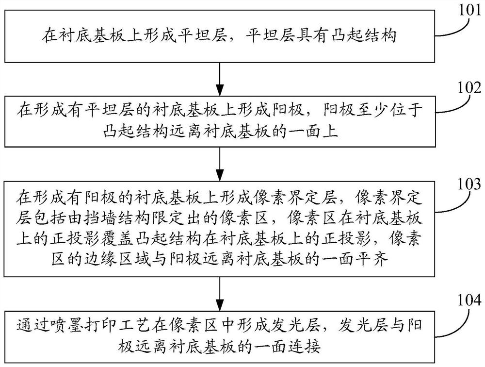
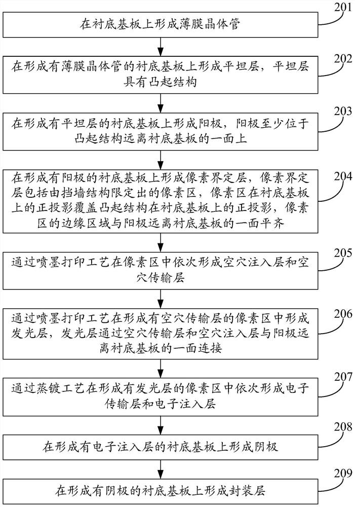
[0047] In order to make the purpose, technical solutions and advantages of the present application clearer, the present application will be further described in detail below with reference to the accompanying drawings. Obviously, the described embodiments are only a part of the embodiments of the present application, rather than all the embodiments. Based on the embodiments in the present application, all other embodiments obtained by those of ordinary skill in the art without creative work fall within the protection scope of the present application.

[0048] The inkjet printing process is a process of printing a solution (also called ink) on the target area (that is, the desired area) through a micron-scale printing nozzle, which has the advantages of simple operation, low cost, simple process and easy realization of large-scale display. With the continuous research and development of high-performance polymer materials and the further improvement of film preparation technology...


PUM


Abstract

The invention discloses a display substrate, a manufacturing method thereof and a display device, and belongs to the technical field of display. The method comprises the following steps: forming a flat layer on a substrate, wherein the flat layer is provided with a convex structure; forming an anode on the substrate on which the flat layer is formed, wherein the anode is at least positioned on one surface, far away from the substrate, of the convex structure; a pixel defining layer is formed on the substrate where the anode is formed, the pixel defining layer comprises a pixel area defined by a retaining wall structure, the orthographic projection of the pixel area on the substrate covers the orthographic projection of the protruding structure on the substrate, and the edge area of the pixel area is flush with the face, away from the substrate, of the anode; and forming a light-emitting layer in the pixel region through an ink-jet printing process, wherein the light-emitting layer is connected with one surface, far away from the substrate, of the anode. The problem that the uniformity of the luminance of the light-emitting layer is poor is solved, and the uniformity of the luminance of the light-emitting layer is improved. The manufacturing method is used for manufacturing the display substrate.

Description

[0001] This application is a divisional application of a Chinese patent application with an application date of April 9, 2019, an application number of 201910281690.5, and an invention title of "display substrate and its manufacturing method, and display device". technical field [0002] The present application relates to the field of display technology, and in particular, to a display substrate, a manufacturing method thereof, and a display device. Background technique [0003] Electroluminescent display devices such as polymer light-emitting diodes (PLED for short) have the advantages of thinness, low power consumption, high contrast ratio, high color gamut and flexible display, and are widely used in the display industry. [0004] Electroluminescent display devices mainly rely on electroluminescent display substrates for display. The electroluminescent display substrate generally includes a base substrate and a thin film transistor (English: Thin Film Transistor; abbrevia...

Claims


Application Information

Patent Timeline
Patent Type & Authority Applications(China)
IPC IPC(8): H01L27/32H01L51/56H01L51/52
CPCH10K59/124H10K71/135H10K50/813H10K59/00
Inventor 崔颖
Owner BOE TECH GRP CO LTD
Why Eureka
Try Eureka