A kind of oled substrate and its preparation method, display device

A substrate and transmittance technology, applied in semiconductor/solid-state device manufacturing, organic semiconductor devices, semiconductor devices, etc., can solve the problems of uneven brightness and uneven light emission of sub-pixels

Active Publication Date: 2021-01-26
BOE TECH GRP CO LTD
View PDF1 Cites 0 Cited by
  • Summary
  • Abstract
  • Description
  • Claims
  • Application Information

AI Technical Summary

Problems solved by technology

On this basis, it will lead to uneven brightness of sub-pixels
For example, for figure 1 In the case of image 3 Non-uniformity of light emission shown

Method used


Image

  • A kind of oled substrate and its preparation method, display device
  • A kind of oled substrate and its preparation method, display device
  • A kind of oled substrate and its preparation method, display device

Examples


Embodiment Construction

[0028] The following will clearly and completely describe the technical solutions in the embodiments of the present invention with reference to the accompanying drawings in the embodiments of the present invention. Obviously, the described embodiments are only some, not all, embodiments of the present invention. Based on the embodiments of the present invention, all other embodiments obtained by persons of ordinary skill in the art without making creative efforts belong to the protection scope of the present invention.

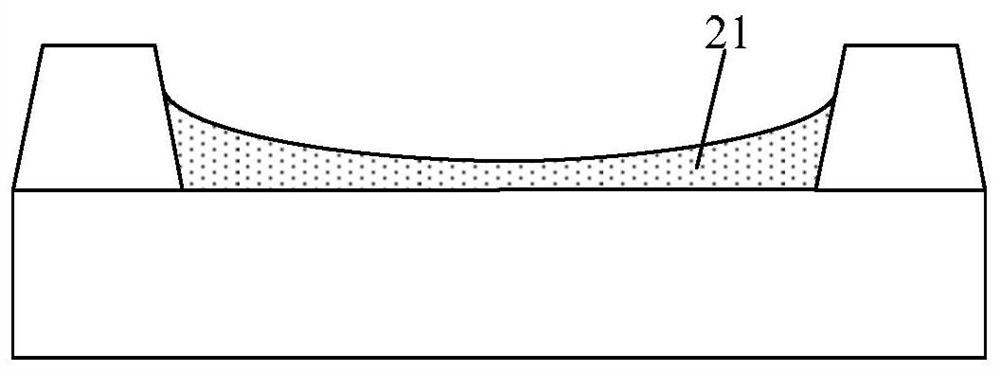
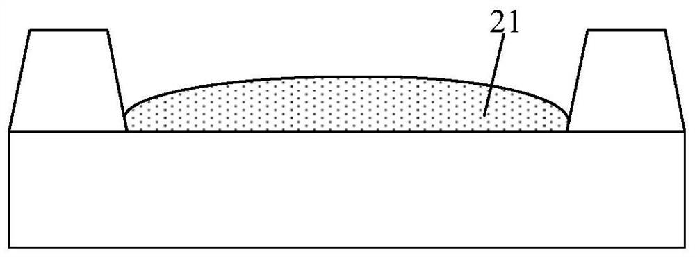
[0029] An embodiment of the present invention provides an OLED substrate, such as Figure 4 and Figure 5 As shown, it includes: a substrate 10, an OLED device 20 disposed on the sub-pixel region on the substrate 10, the thickness of the middle region of the organic layer 21 of the OLED device is different from that of the edge region; further, the OLED substrate also includes a substrate disposed on the substrate The transmittance adjustment layer 30 in the ...


PUM


Abstract

Embodiments of the present invention provide an OLED substrate, a manufacturing method thereof, and a display device, which relate to the field of display technology and can improve uniformity of light emission. An OLED substrate, comprising: a substrate, an OLED device arranged in a sub-pixel region on the substrate, the thickness of the middle region of the organic layer of the OLED device is different from that of the edge region; The transmittance adjustment layer in the sub-pixel area on the substrate and located on the light-emitting side of the organic layer, the transmittance of the transmittance adjustment layer corresponding to the thicker region of the organic layer is greater than that corresponding to the thickness of the organic layer Transmittance in thinner regions.

Description

technical field [0001] The invention relates to the field of display technology, in particular to an OLED substrate, a preparation method thereof, and a display device. Background technique [0002] Compared with Liquid Crystal Display (LCD), Organic Light-Emitting Diode (OLED) display has the advantages of self-illumination, fast response, wide viewing angle, high brightness, bright color, light and thin, etc. A generation of display technology. [0003] The organic layer preparation methods of each sub-pixel in an OLED display mainly include vacuum evaporation and solution processing. Vacuum evaporation is suitable for small organic molecules. The film formation is uniform and the technology is relatively mature, but the investment in equipment is large, the utilization rate of materials is low, and the alignment accuracy of large-size products is low. Solution process, including spin coating, inkjet printing, nozzle coating method, etc., is suitable for polymer material...

Claims


Application Information

Patent Timeline
Patent Type & Authority Patents(China)
IPC IPC(8): H01L27/32H01L51/52H01L51/56
CPCH10K59/00H10K50/30H10K71/00H10K59/38H10K59/122H10K50/85H10K2102/351H10K50/858H10K59/126H10K71/135H10K2102/3035
Inventor 胡春静
Owner BOE TECH GRP CO LTD
Why Eureka
Try Eureka