AC plasma display panel
A plasma and display panel technology, applied in the direction of static indicators, gas discharge electrodes, tube structure components, etc., can solve the unfavorable adjustment of X and Y electrode spacing, increase the spacing of partition walls 6, and affect the phosphor Visible light luminous efficiency and other issues
- Summary
- Abstract
- Description
- Claims
- Application Information
AI Technical Summary
Problems solved by technology
Method used
Image

Examples
Embodiment Construction
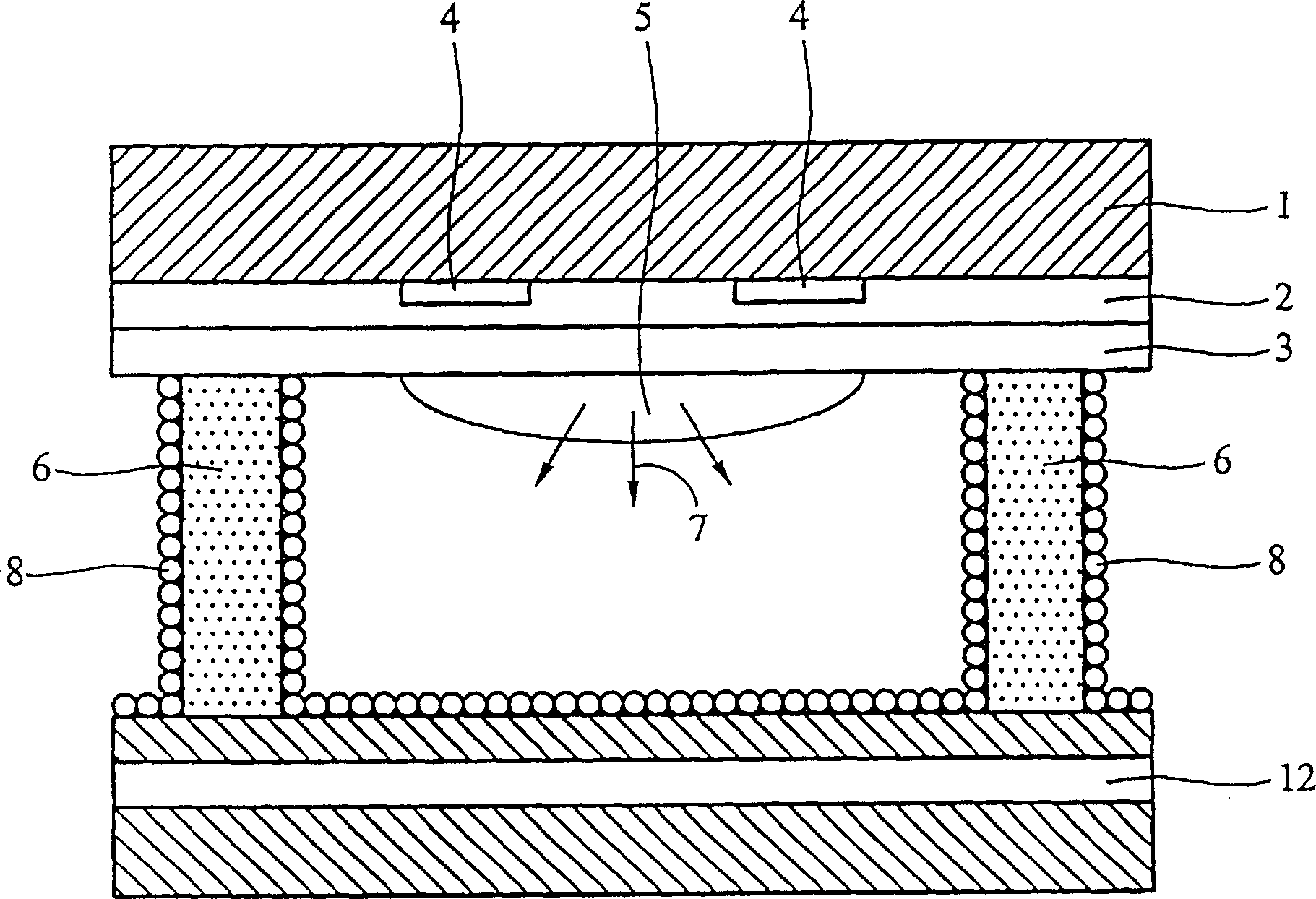
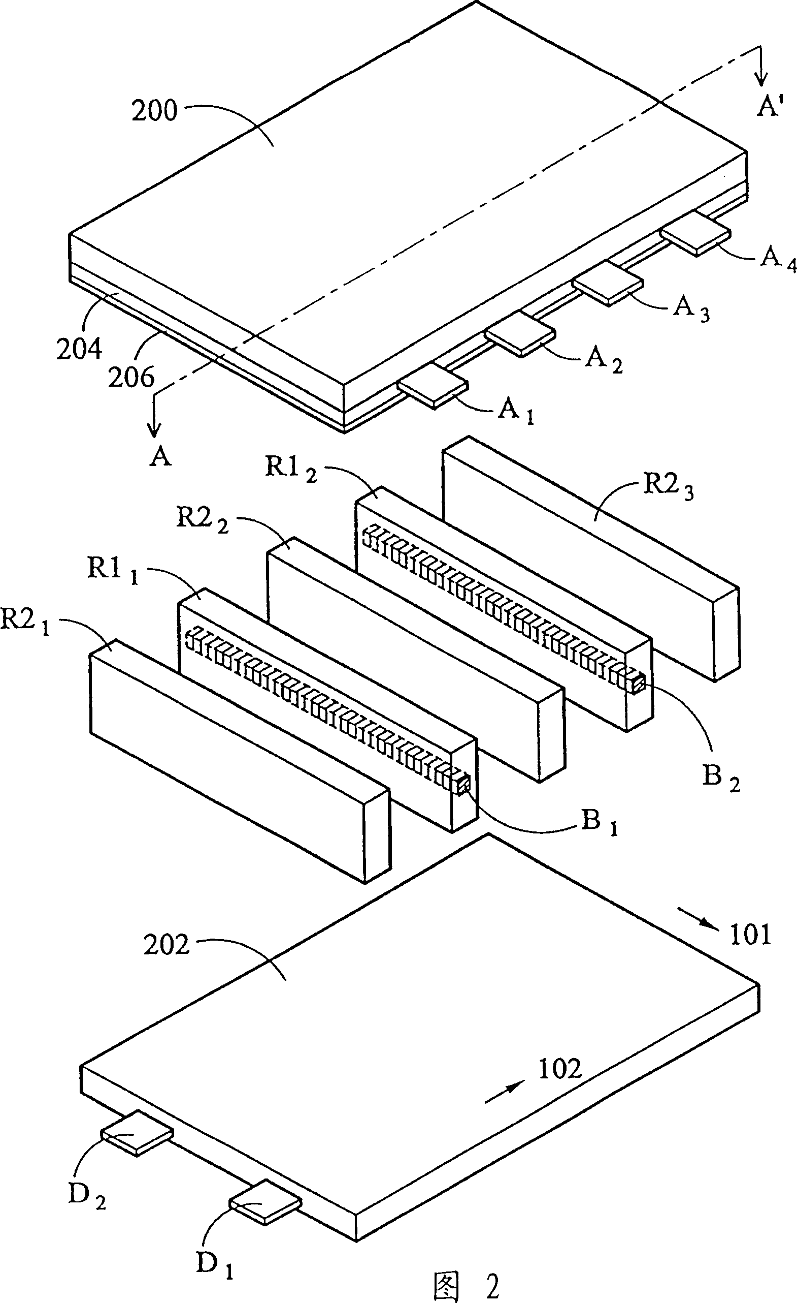
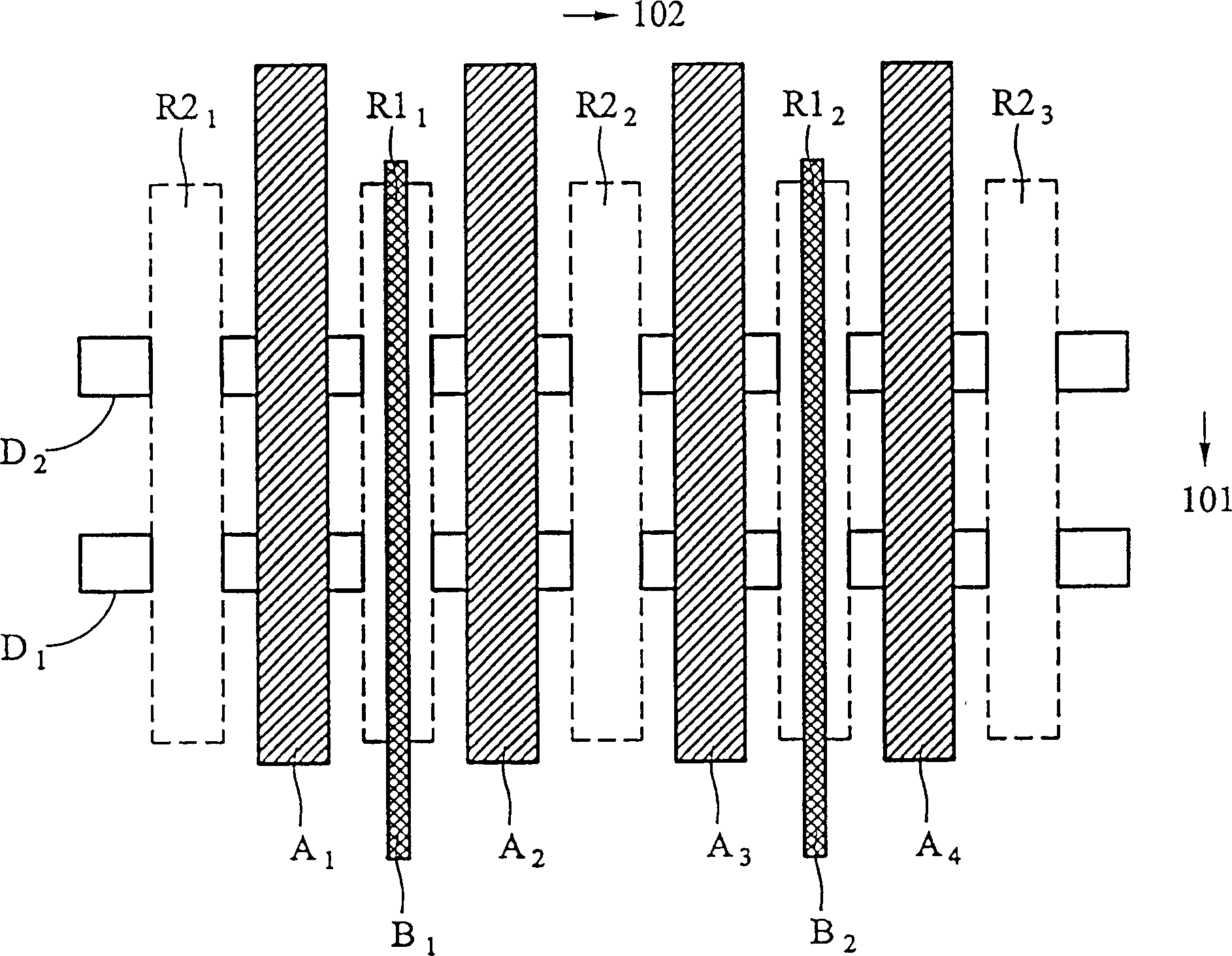
[0051] FIG. 2 is a schematic diagram showing the structure of the AC plasma display panel of the present invention. image 3 It is a plan view showing the electrode arrangement of the AC plasma display panel shown in FIG. 2 .
[0052] Referring to Fig. 2, the AC plasma display panel of the present invention includes: a first substrate (front glass substrate) 200; a first electrode (A i , i=1~4), which is arranged on the first substrate 200 along the first direction 101; a second substrate (rear glass substrate) 202, which is arranged parallel to the first substrate 201 so that the first A discharge space is formed between the substrate 200 and the second substrate 202; a first strip-shaped partition wall (R1 j , j=1~2) and a second strip partition wall (R2 k , k=1~3), they are arranged in the discharge space parallel to each other along the first direction 101 and interlaced with each other; a third electrode (D m , m=1˜2), disposed on the second substrate 202 along the sec...
PUM
 Abstract
Description
Claims
Application Information
 - Generate Ideas
- Intellectual Property
- Life Sciences
- Materials
- Tech Scout
- Unparalleled Data Quality
- Higher Quality Content
- 60% Fewer Hallucinations
Browse by: Latest US Patents, China's latest patents, Technical Efficacy Thesaurus, Application Domain, Technology Topic, Popular Technical Reports.
© 2025 PatSnap. All rights reserved.Legal|Privacy policy|Modern Slavery Act Transparency Statement|Sitemap|About US| Contact US: help@patsnap.com