Semiconductor device

A semiconductor and device technology, applied in the field of high-performance semiconductor devices, can solve problems such as voltage drop of semiconductor chips that cannot be solved, and achieve the effect of increasing the number of connection terminals, reducing voltage drop, and improving installation efficiency

Inactive Publication Date: 2002-07-17
KK TOSHIBA
View PDF0 Cites 5 Cited by
  • Summary
  • Abstract
  • Description
  • Claims
  • Application Information

AI Technical Summary

Problems solved by technology

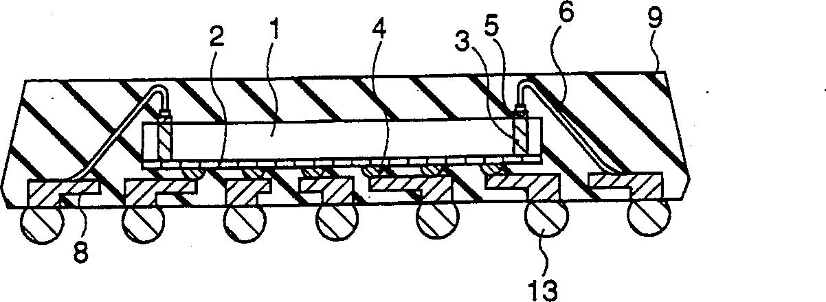
[0006] However, in the case of such a package structure, when supplementing the power supply, since the circuit formation surfaces of the semiconductor chips face each o

Method used


Image

  • Semiconductor device
  • Semiconductor device
  • Semiconductor device

Examples


Example

[0080] [First Embodiment]

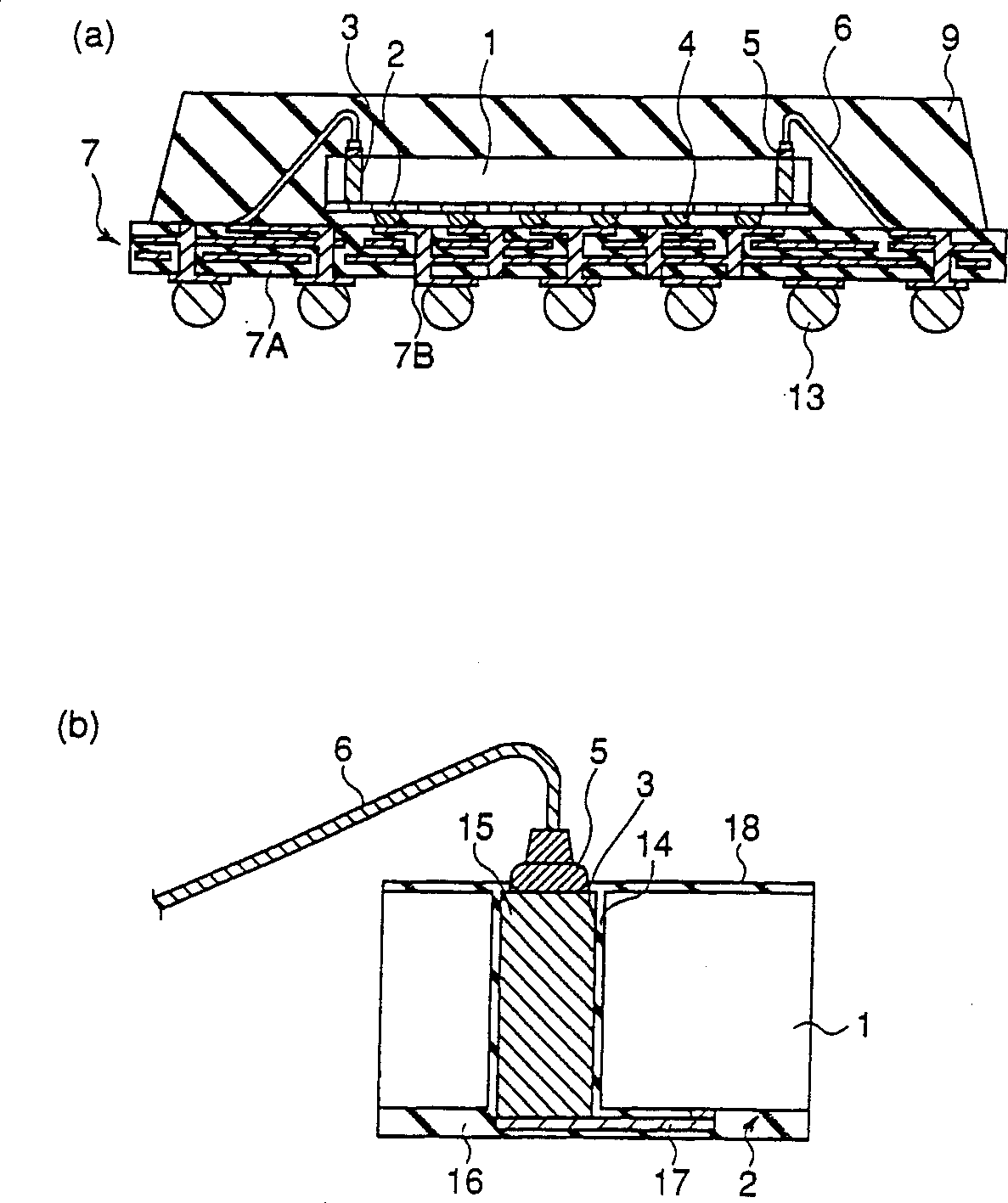
[0081] figure 1 (a) and (b) respectively illustrate the semiconductor device of the first embodiment of the present invention, (a) is a schematic cross-sectional view, and (b) is a partial enlarged view of (a). As shown in Figure (a), the semiconductor chip 1 is mounted with the formation surface 2 of the semiconductor element (internal circuit) facing the wiring board 7 (face down). The formation surface 2 of the semiconductor element is formed by dispersing connection terminals (conductive bumps) 4 over the entire area (for example, in an array), and is electrically connected to the wiring layer 7B of the wiring board 7 via the connection terminals 4. The wiring board 7 has wiring layers (multilayer wiring) 7B formed on both sides and inside of an insulating substrate 7A made of resin or the like, respectively, and the wiring layer is arranged on the stern corresponding to the bump 4 on the mounting side of the semiconductor chip 1 . The wiring laye...

Example

[0087] [Second embodiment]

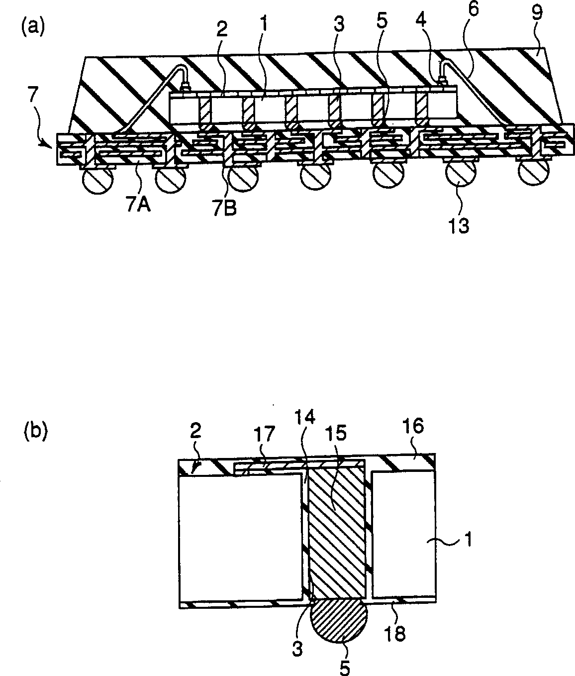
[0088] figure 2 (a) and (b) respectively illustrate the semiconductor device of the second embodiment of the present invention, (a) is a schematic cross-sectional view, and (b) is a partially enlarged view of (a). In the second embodiment, the semiconductor chip 1 is mounted with the back surface of the semiconductor element forming surface 2 facing the wiring board 7 (face upward). The through holes 3 in which the conductive member 15 is embedded are dispersedly arranged throughout the semiconductor chip 1, and connection terminals (conductive bumps) 5 formed on the back surface of the chip 1 through the through holes 3 are used to connect to the wiring board 7. A connecting terminal (bump) 4 similar to a general semiconductor device is formed on the outer periphery of the semiconductor element forming surface 2 of the semiconductor chip 1, and the connecting terminal 4 is electrically connected to the wiring layer 7B of the wiring board 7 via wire ...


PUM


Abstract

A semiconductor device is disclosed, which comprise a first semiconductor chip where a semiconductor element is formed, a first connecting terminal arranged on a semiconductor element formation surface side in the first semiconductor chip and connected electrically to the semiconductor element, a conductive member buried in a through hole that goes through the first semiconductor chip, a second connecting terminal arranged on a back surface side of the semiconductor element formation surface in the first semiconductor chip, and connected electrically to the semiconductor element via the conductive member, a wiring substrate to which the first semiconductor chip is mounted, and a third connecting terminal at least portion of which is formed at a position corresponding to one of the first connecting terminal and the second connecting terminal, and which is electrically connected to the one of the first connecting terminal and the second connecting terminal.

Description

technical field [0001] The present invention relates to a semiconductor device with a packaging structure in which through holes for embedding conductive components are formed in a semiconductor chip, and wiring is drawn out from the formation surface side and the back side of the semiconductor element, especially a high-performance semiconductor device with enhanced power supply. Background technique [0002] With the reduction of power supply voltage and the increase of circuit scale accompanying the refinement of semiconductor integrated circuits, the size of semiconductor chips has been increased, and the problem of voltage drop inside the semiconductor chip has become prominent. As a countermeasure against this, a package of a flip-chip structure in which connection terminals are provided across the entire surface of a semiconductor chip and connected face down on a multilayer wiring board is becoming mainstream. [0003] Figure 29 is a cross-sectional view showing a s...

Claims


Application Information

Patent Timeline
IPC IPC(8): H01L23/12H01L21/768H01L23/31H01L23/48H01L23/52H01L25/065H01L25/07H01L25/18
CPCH01L2224/73257H01L2224/73265H01L2924/15153H01L2224/16245H01L2924/12041H01L25/0657H01L2224/16H01L2225/06586H01L2224/16225H01L2924/01004H01L2225/06506H01L2225/06589H01L2924/1517H01L2225/06582H01L2224/48145H01L24/48H01L2225/0651H01L2924/14H01L2924/15311H01L24/73H01L2924/18161H01L2924/01005H01L2224/32145H01L2924/01082H01L23/3107H01L2924/01013H01L2225/06568H01L2225/06541H01L2924/01029H01L2224/13025H01L2224/16145H01L2225/06513H01L2924/1532H01L2224/48227H01L23/481H01L2924/01033H01L2924/00014H01L2224/02372H01L2224/0401H01L2224/13024H01L2924/181H01L2224/45099H01L2924/00H01L2924/00012H01L23/12
Inventor 杉崎吉昭
Owner KK TOSHIBA
Why Eureka
Try Eureka