

Semiconductor device
A semiconductor and device technology, applied in the field of high-performance semiconductor devices, can solve problems such as the voltage drop of semiconductor chips that cannot be solved, and achieve the effects of increasing the number of connection terminals, reducing the voltage drop, and improving the installation efficiency
- Summary
- Abstract
- Description
- Claims
- Application Information
AI Technical Summary
Problems solved by technology
Method used
Image

Examples
no. 1 Embodiment
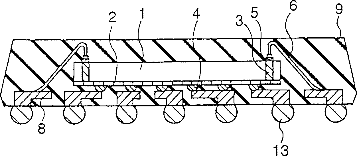
[0081] figure 1 (a) and (b) respectively illustrate the semiconductor device of the first embodiment of the present invention, (a) is a schematic cross-sectional view, and (b) is a partial enlarged view of (a). As shown in Figure (a), the semiconductor chip 1 is mounted with the formation surface 2 of the semiconductor element (internal circuit) facing the wiring board 7 (face down). The formation surface 2 of the semiconductor element is formed by dispersing connection terminals (conductive bumps) 4 over the entire area (for example, in an array), and is electrically connected to the wiring layer 7B of the wiring board 7 via the connection terminals 4. The wiring board 7 has wiring layers (multilayer wiring) 7B formed on both sides and inside of an insulating substrate 7A made of resin or the like, respectively, and the wiring layer is arranged on the stern corresponding to the bump 4 on the mounting side of the semiconductor chip 1 . The wiring layer 7B is led out to the back ...
no. 2 Embodiment
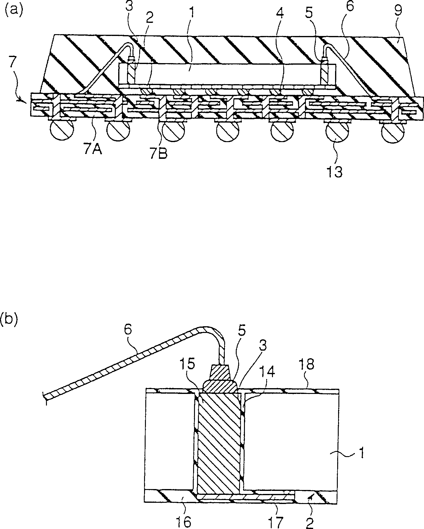
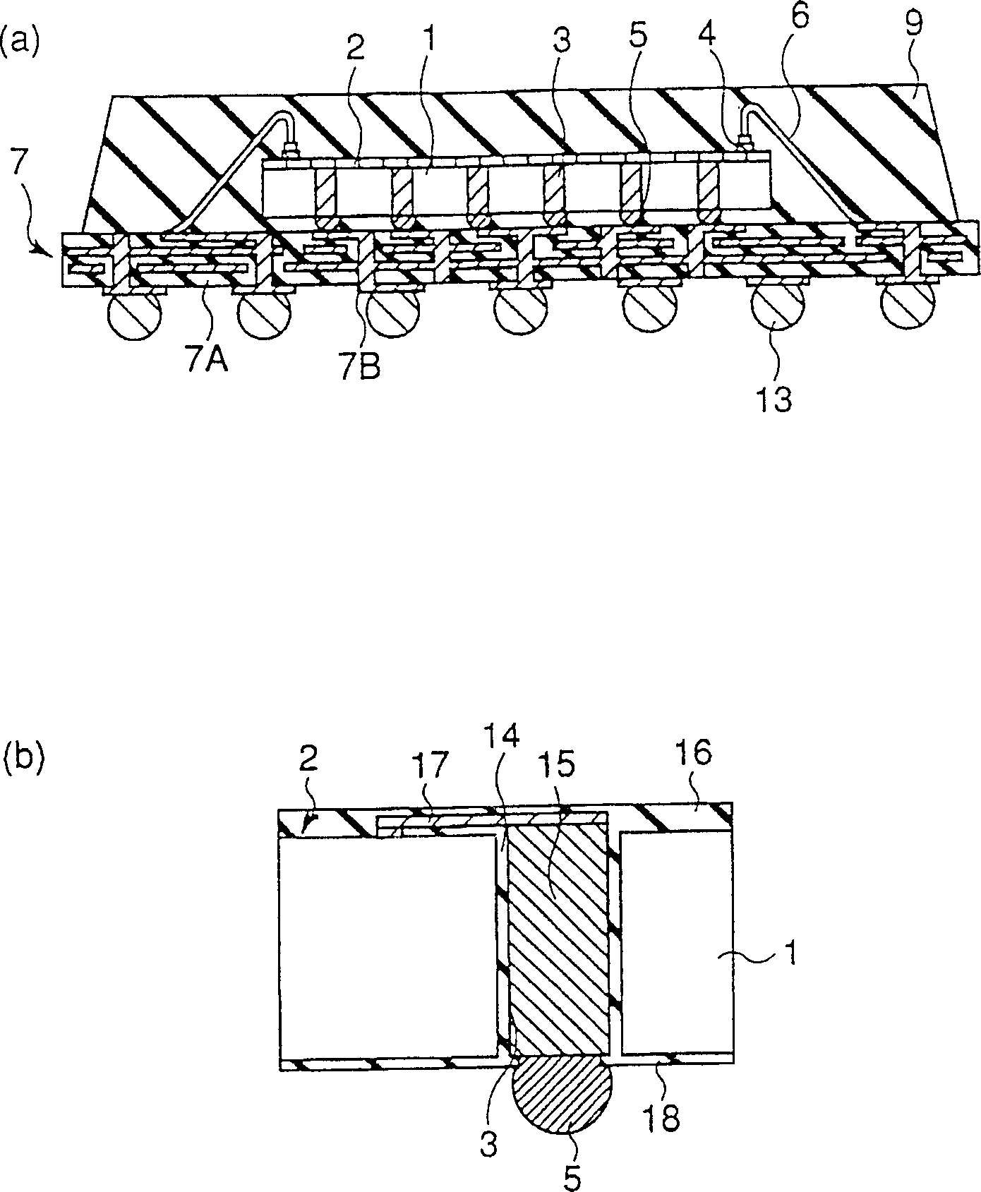
[0088] figure 2 (a) and (b) respectively illustrate the semiconductor device of the second embodiment of the present invention, (a) is a schematic cross-sectional view, and (b) is a partially enlarged view of (a). In the second embodiment, the semiconductor chip 1 is mounted with the back surface of the semiconductor element forming surface 2 facing the wiring board 7 (face upward). The through holes 3 in which the conductive member 15 is embedded are dispersedly arranged throughout the semiconductor chip 1, and connection terminals (conductive bumps) 5 formed on the back surface of the chip 1 through the through holes 3 are used to connect to the wiring board 7. A connecting terminal (bump) 4 similar to a general semiconductor device is formed on the outer periphery of the semiconductor element forming surface 2 of the semiconductor chip 1, and the connecting terminal 4 is electrically connected to the wiring layer 7B of the wiring board 7 via wire bonding.
[0089] In the abov...
PUM
 Abstract
Description
Claims
Application Information