

Cutting making process of silicon carbide boat for chip manufacture
A technology of silicon carbide boat and manufacturing method, which is applied in semiconductor/solid-state device manufacturing, metal processing, electrical components, etc., can solve the problems of high processing cost, high cost, high damage rate, etc., and achieve high precision, high production efficiency, The effect of low breakage rate
- Summary
- Abstract
- Description
- Claims
- Application Information
AI Technical Summary
Problems solved by technology
Method used
Image

Examples
Embodiment Construction
[0010] The present invention will be further described in detail below in conjunction with the accompanying drawings and embodiments.
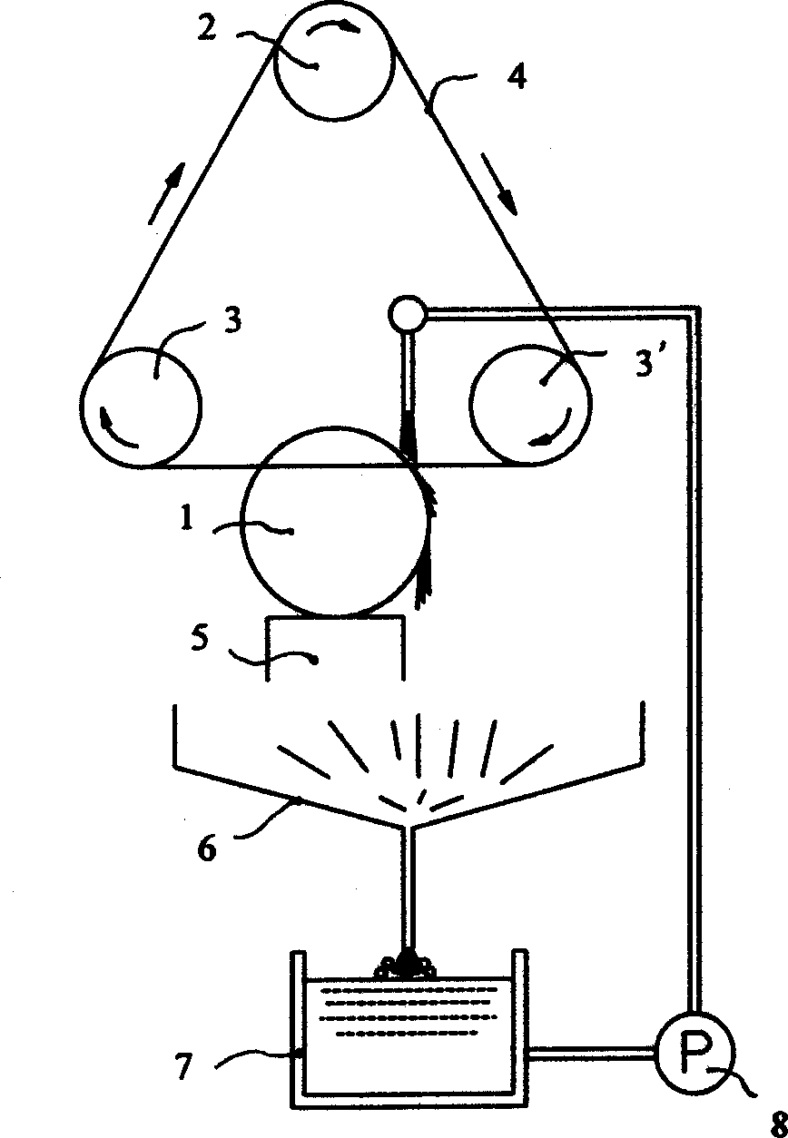
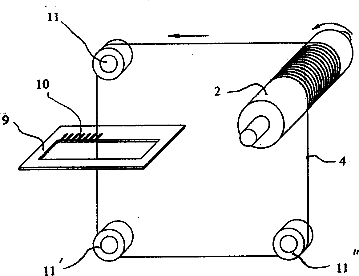
[0011] first embodiment, figure 1 Shown is the schematic diagram of the wire cutting processing equipment and technology that the present invention is used for processing and manufacturing the silicon carbide boat that semiconductor wafer is used, and workpiece 1 is clamped on the workbench by fixture, and the cutting that is made up of a roller and two guide wheels Wire drive train, that roller on the top is the winding driving roller 2, and guide wheels 3, 3' can regulate the tension of cutting line 4. The core wire of the cutting wire 4 is a tungsten-molybdenum wire, and the outer part includes corundum powder coating. The particle size of described corundum powder is 260 grains / cm 2 , the hardness of the diamond powder is 10 on the Mohs scale. The cutting line 4 is wound on the drive roller 2 (see figure 2 ), the rotational speed of t...
PUM
 Abstract
Description
Claims
Application Information