
Display device

A display device, field emission technology, applied in the direction of image/graphic display tube, electrode device and related components, discharge lamp, etc., can solve problems such as electron beam divergence

Inactive Publication Date: 2006-01-25
KONINK PHILIPS ELECTRONICS NV +1
View PDF3 Cites 2 Cited by
  • Summary
  • Abstract
  • Description
  • Claims
  • Application Information

AI Technical Summary

Problems solved by technology

Lowering the anode voltage does not help with this challenge as it causes the electron beam to diverge, which is undesirable in display devices

Method used


Image

  • Display device
  • Display device
  • Display device

Examples


Embodiment Construction

[0028] Description of preferred embodiments

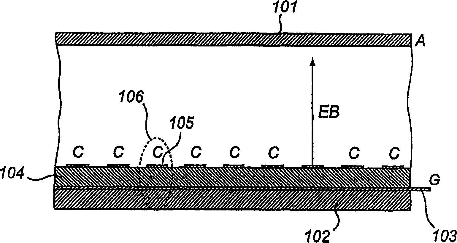
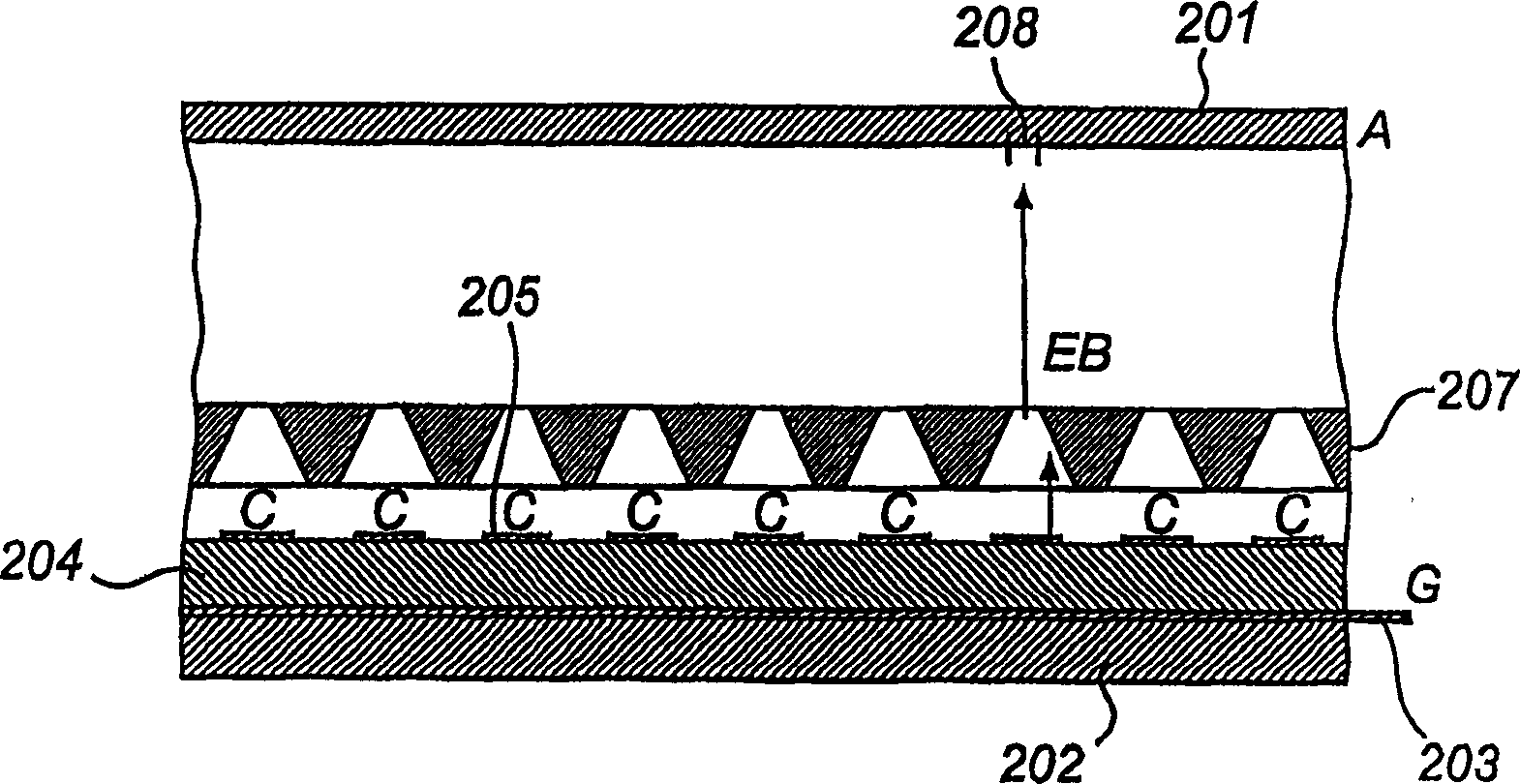
[0029] Figure 1 shows a cross-sectional view of a display device according to the prior art. The first substrate 101 is used as a display screen and connected to the anode (A). A plurality of gate electrodes 103 are disposed on the second substrate 102, and only a section of one of the gate electrodes is shown in the figure. An insulating layer 104 is provided on the gate electrode to isolate the gate electrode 103 from a plurality of cathodes (C) formed on the insulating layer 104 . The cathodes 105 are striped and extend in a direction perpendicular to the gate electrode strips 103 . An emission unit 106 is provided at the intersection of the grid electrode strip 103 and the cathode strip 105, so that the grid electrode 103 can be used to control electron emission from the cathode 105 in the area of ​​the emission unit 106. This emitter structure can be called under-gate emitter. Since the gate electrode is placed under the ca...


PUM


Abstract

The invention relates to a display device having under-gate emitters, i.e. emitters where the gates (203) are arranged under the cathodes (205), beneath an insulating layer (204). In order to protect the emitters from a high electric field from an anode (A), an electron guidance element (207) is placed between the emitters and the anode. This allows a relatively low voltage swing to be used for controlling the electron emission from the emitters from the on-state to the off-state.

Description

technical field [0001] The invention relates to a display device, which is composed of two parallel planar substrates which are separated and have a certain distance. An anode is made on the first substrate, and many cathodes are made on a plane of the second substrate facing the first substrate. On a plane of the second substrate, there are many grid electrodes under the cathodes, these grid electrodes are separated from the cathodes by an electric insulating layer, and they are used to control the electron emission of the cathodes. Background of the invention [0002] The field reflective structure is described in detail in US Patent 6,420,726. In this structure, the gate electrode is formed as a set of parallel strips on the substrate, and a continuous layer of insulating material is provided on the gate electrode. The cathode is formed on the insulating layer as parallel strips, and the cathode parallel strips are perpendicular to the gate electrode parallel strips. S...

Claims


Application Information

Patent Timeline
Patent Type & Authority Applications(China)
IPC IPC(8): H01J31/12H01J29/46H01J29/48
CPCH01J2329/46H01J31/127H01J29/482H01J29/467
Inventor W·A·J·A·范德波尔T·范祖芬H·A·维伦加J·P·A·迪本E·C·科斯曼M·F·吉尔利斯
Owner KONINK PHILIPS ELECTRONICS NV
Learn More