Chip package circuit board module

a technology of circuit board and chip, applied in the field of circuit board modules, can solve the problems of circuit board reliability decline, pad damage on the circuit board, circuit board board damage, etc., and achieve the effect of high yield and quick and easy configuration

Active Publication Date: 2018-08-21
UNIMICRON TECH CORP
View PDF5 Cites 3 Cited by
  • Summary
  • Abstract
  • Description
  • Claims
  • Application Information

AI Technical Summary

Benefits of technology

[0004]The invention is directed to a chip package circuit board module, where a substitution chip is adapted to be quickly and easily configured on the circuit board to achieve a high yield.

Problems solved by technology

However, when the LED chip is damaged, the package is failed, or the LED chip cannot emit light due to other reasons, it is required to disassemble the LED chip to clean pads on the circuit board, and sometimes re-soldering is required, and then a new LED chip is packaged.
However, the aforementioned rework process probably encounters following problems: when the LED chip is stripped, copper lines on a surface of the circuit board are probably stripped together; a high temperature is probably applied during the process of stripping the LED chip, though under a high temperature environment, the circuit board may have unexpected expansion or shrink, which probably damages the circuit board, such that reliability of the circuit board is decreased; when the LED chip is stripped, the pads on the circuit board are probably damaged, and the new LED chip packaged at the same position probably has a problem of yield reduction.

Method used


Image

  • Chip package circuit board module
  • Chip package circuit board module
  • Chip package circuit board module

Examples


Embodiment Construction

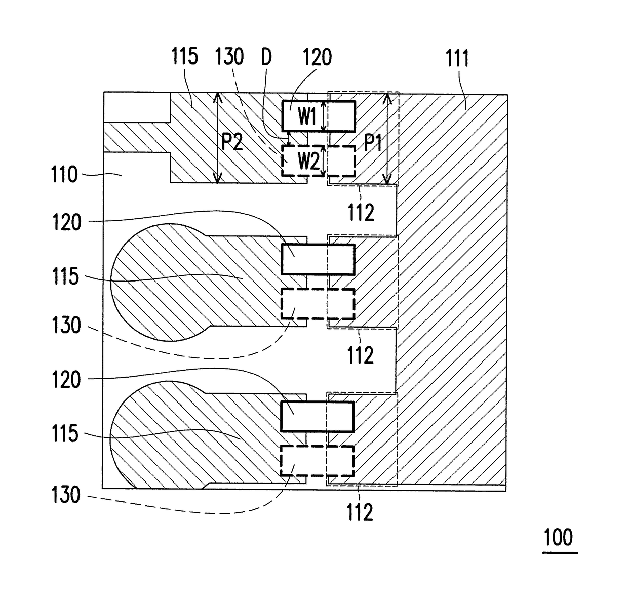
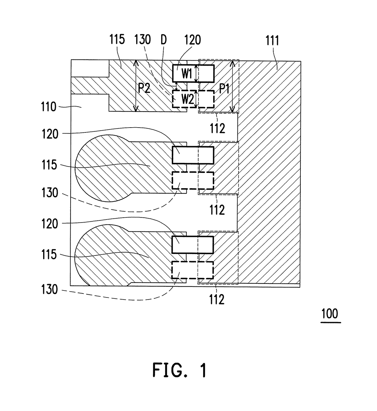
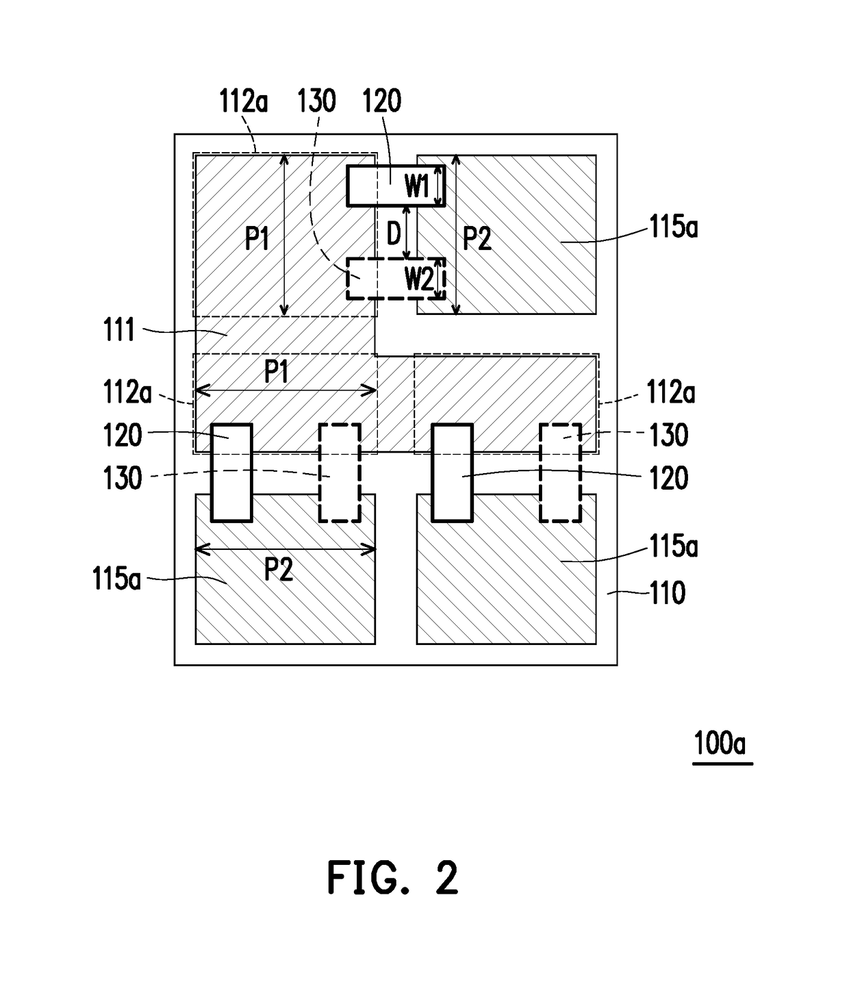
[0020]FIG. 1 is a schematic diagram of a chip package circuit board module according to an embodiment of the invention. Referring to FIG. 1, the chip package circuit board module 100 of the present embodiment includes a circuit board 110 and a plurality of original chips 120. The circuit board 110 includes a plurality of first pads 112 and a plurality of second pads 115. In the present embodiment, the original chips 120 are, for example, light-emitting diode (LED) chips, though the type of the original chips 120 is not limited thereto. Moreover, in the present embodiment, numbers of the original chips 120, the first pads 112 and the second pads 115 are, for example, respectively three, though the numbers of the original chips 120, the first pads 112 and the second pads 115 are not limited thereto. According to FIG. 1, the first pads 112 are connected through a connection portion 111, though in other embodiments, the first pads 112 can also be separated from each other according to a...


PUM


Abstract

A chip package circuit board module includes a circuit board and an original chip. The circuit board includes a first pad and a second pad disposed besides the first pad and separated from the first pad. The original chip is connected to the first pad and the second pad. A width of the original chip is W1, a total width of the first pad is P1, and a total width of the second pad is P2. The total width P1 of the first pad is larger than twice of the width W1 of the original chip, and the total width P2 of the second pad is larger than twice of the width W1 of the original chip.

Description

BACKGROUND OF THE INVENTIONField of the Invention[0001]The invention relates to a circuit board module, and particularly relates to a chip package circuit board module.Description of Related Art[0002]Generally, a circuit board module of a light-emitting diode (LED) chip is to package the LED chip on a circuit board. However, when the LED chip is damaged, the package is failed, or the LED chip cannot emit light due to other reasons, it is required to disassemble the LED chip to clean pads on the circuit board, and sometimes re-soldering is required, and then a new LED chip is packaged.[0003]However, the aforementioned rework process probably encounters following problems: when the LED chip is stripped, copper lines on a surface of the circuit board are probably stripped together; a high temperature is probably applied during the process of stripping the LED chip, though under a high temperature environment, the circuit board may have unexpected expansion or shrink, which probably dam...

Claims


Application Information

Patent Timeline
Patent Type & Authority Patents(United States)
IPC IPC(8): H01L25/075H01L23/498
CPCH01L25/0753H01L23/49811H01L33/62
Inventor LIU, WEN-FANGLEE, SHAO-CHIENTSENG, CHEN-WEILI, ZONG-HUA
Owner UNIMICRON TECH CORP
Why Eureka
Try Eureka