Electronic circuit module
a technology of electronic circuit module and circuit board, applied in the direction of printed circuit aspects, cross-talk/noise/interference reduction, magnetic/electric field screening, etc., can solve the problems of difficult to obtain a predetermined joining strength and formation of pin holes, so as to prevent the rise of metal covers and reduce the occurrence of pin holes
- Summary
- Abstract
- Description
- Claims
- Application Information
AI Technical Summary
Benefits of technology
Problems solved by technology
Method used
Image

Examples
first embodiment
[0055 of Cover-Fixing Method for Electronic Circuit Module
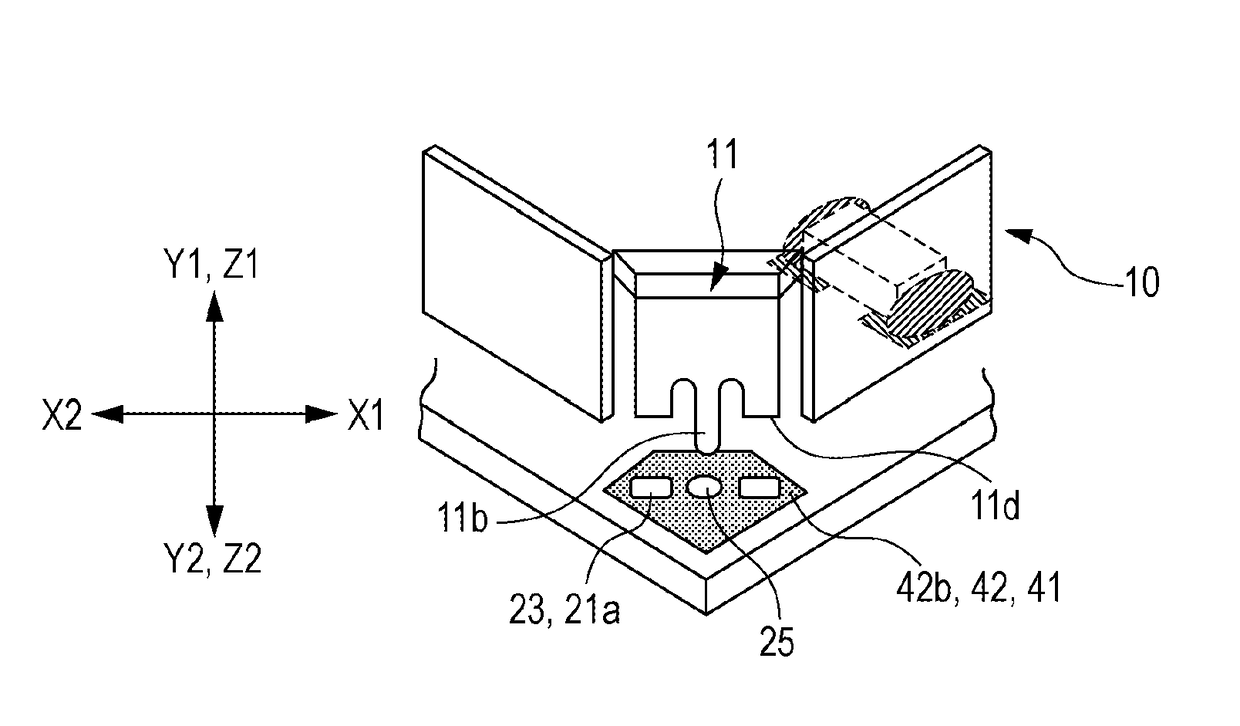
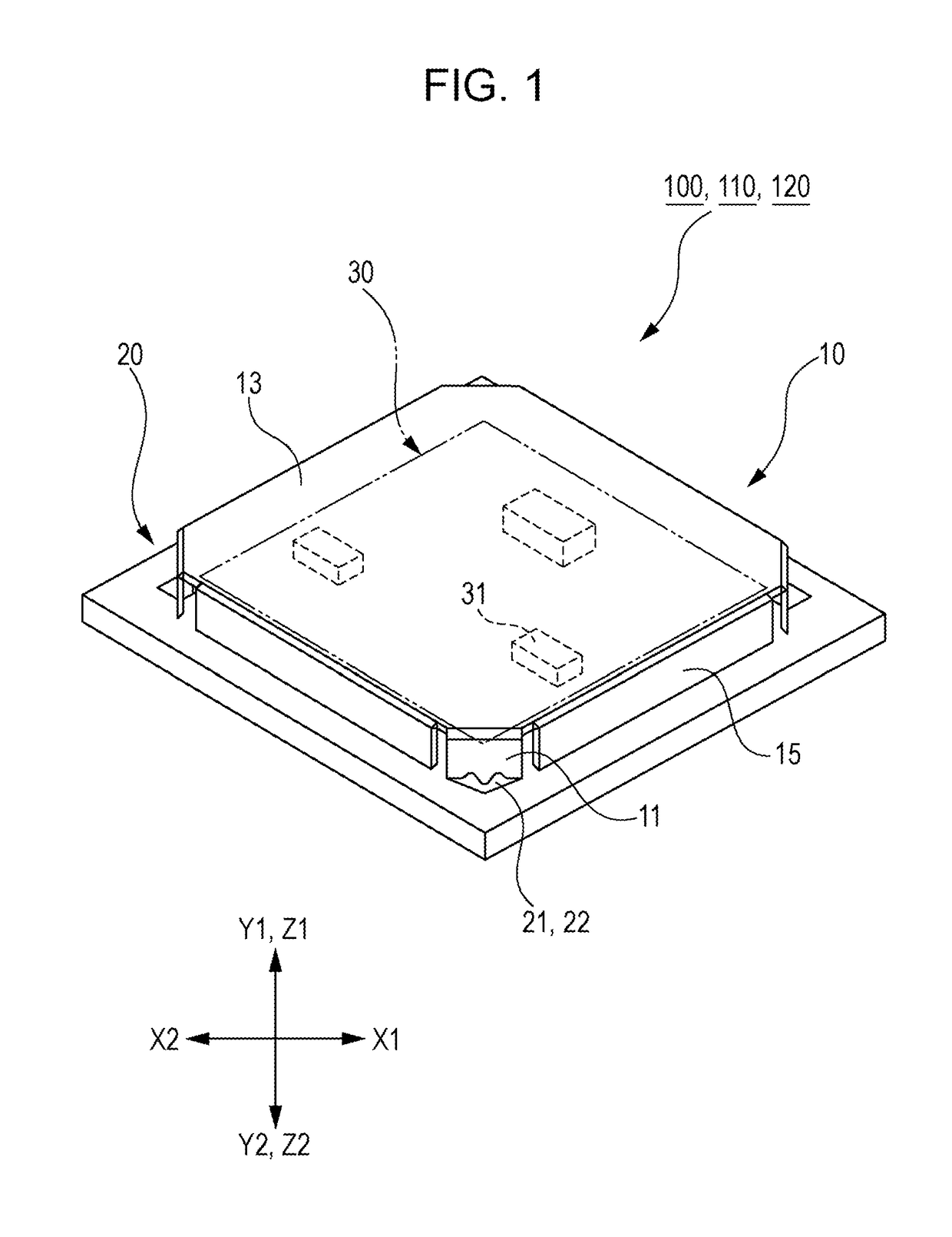
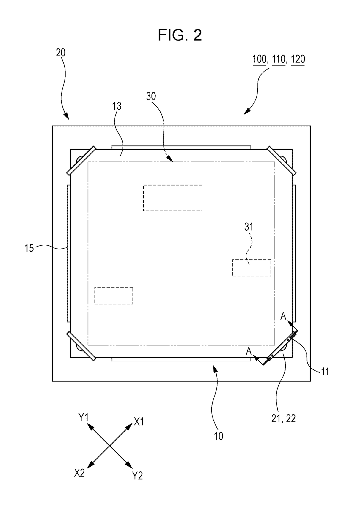
[0056]A first embodiment of a cover-fixing method for an electronic circuit module according to the present invention will be described with reference to FIGS. 1, 2, 3, 4 and 9A to 9C. FIGS. 9A to 9C are schematic diagrams illustrating the first embodiment of the cover-fixing method for the electronic circuit module viewed along line A-A in FIG. 2. FIG. 9A is a schematic diagram illustrating the state before first reflow in a mounting step. FIG. 9B is a schematic diagram illustrating the state before second reflow in an assembly step. FIG. 9C is a schematic diagram illustrating the state after the second reflow. FIG. 4 is an enlarged schematic view illustrating the state in which the joining material layer 42 is formed and the metal cover 10 is inserted before the second reflow.
[0057]The first embodiment of the cover-fixing method for the electronic circuit module is a cover-fixing method for the above-described electronic ci...
second embodiment
[0065 of Cover-Fixing Method for Electronic Circuit Module
[0066]A second embodiment of a cover-fixing method for an electronic circuit module according to the present invention will be described with reference to FIGS. 1, 2, 3, 10A to 10C, and 11. FIGS. 10A to 10C are schematic diagrams illustrating the second embodiment of the cover-fixing method for the electronic circuit module viewed along line A-A in FIG. 2. FIG. 10A is a schematic diagram illustrating the state before first reflow in a mounting step. FIG. 10B is a schematic diagram illustrating the state before second reflow in an assembly step. FIG. 10C is a schematic diagram illustrating the state after the second reflow. FIG. 11 is an enlarged schematic view illustrating the state in which the joining material layer 42 is formed and the metal cover 10 is inserted before the second reflow.
[0067]The second embodiment of the cover-fixing method for the electronic circuit module is a cover-fixing method for the above-described ...
third embodiment
[0073 of Cover-Fixing Method for Electronic Circuit Module
[0074]A third embodiment of a cover-fixing method for an electronic circuit module according to the present invention will be described with reference to FIGS. 1, 2, 7, 8, and 12A to 12C. FIGS. 12A to 12C are schematic diagrams illustrating the third embodiment of the cover-fixing method for the electronic circuit module viewed along line A-A in FIG. 2. FIG. 12A is a schematic diagram illustrating the state before first reflow in a mounting step. FIG. 12B is a schematic diagram illustrating the state before second reflow in an assembly step. FIG. 12C is a schematic diagram illustrating the state after the second reflow. FIG. 8 is an enlarged schematic view illustrating the state in which the joining material layer 42 is formed and the metal cover 10 is inserted before the second reflow.
[0075]The third embodiment of the cover-fixing method for the electronic circuit module is a cover-fixing method for the electronic circuit mo...
PUM
 Abstract
Description
Claims
Application Information
 - R&D
- Intellectual Property
- Life Sciences
- Materials
- Tech Scout
- Unparalleled Data Quality
- Higher Quality Content
- 60% Fewer Hallucinations
Browse by: Latest US Patents, China's latest patents, Technical Efficacy Thesaurus, Application Domain, Technology Topic, Popular Technical Reports.
© 2025 PatSnap. All rights reserved.Legal|Privacy policy|Modern Slavery Act Transparency Statement|Sitemap|About US| Contact US: help@patsnap.com