Apparatus and method for reducing wafer warpage

a technology of apparatus and wafer, applied in the direction of semiconductor/solid-state device testing/measurement, semiconductor device details, semiconductor/solid-state device testing/measurement, etc., can solve the problems of wafer warpage, wafer might not be fixed to equipment, and may occur, so as to reduce the effect of wafer warpag

Active Publication Date: 2019-03-19
SAMSUNG ELECTRONICS CO LTD
View PDF28 Cites 1 Cited by
  • Summary
  • Abstract
  • Description
  • Claims
  • Application Information

AI Technical Summary

Benefits of technology

[0004]An exemplary embodiment of the present inventive concept provides an apparatus for reducing wafer warpage.
[0005]An exemplary embodiment of the present inventive concept provides a method for reducing wafer warpage.

Problems solved by technology

A wafer might not be fixed to equipment during assembly and test processes and thus wafer warpage may occur after a mold process.
Wafer warpage may result from a difference in respective thermal expansion coefficients of a film material, a mold material, and a stack structure bonding material of a silicon device.

Method used


Image

  • Apparatus and method for reducing wafer warpage
  • Apparatus and method for reducing wafer warpage
  • Apparatus and method for reducing wafer warpage

Examples


Embodiment Construction

[0025]An apparatus for reducing wafer warpage according to some exemplary embodiments of the present inventive concept will be described in more detail below with reference to FIGS. 1 to 5.

[0026]FIG. 1 is a front view illustrating an apparatus for reducing wafer warpage according to an exemplary embodiment of the present inventive concept. FIG. 2 is a top view illustrating the apparatus for reducing wafer warpage of FIG. 1. FIG. 3 is a diagram illustrating the apparatus for reducing wafer warpage of FIG. 1. FIG. 4 is a front view illustrating operation of the apparatus for reducing wafer warpage of FIG. 1. FIG. 5 is a front view illustrating operation of the apparatus for reducing wafer warpage of FIG. 1.

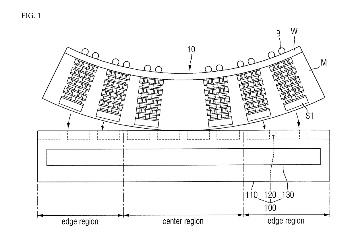
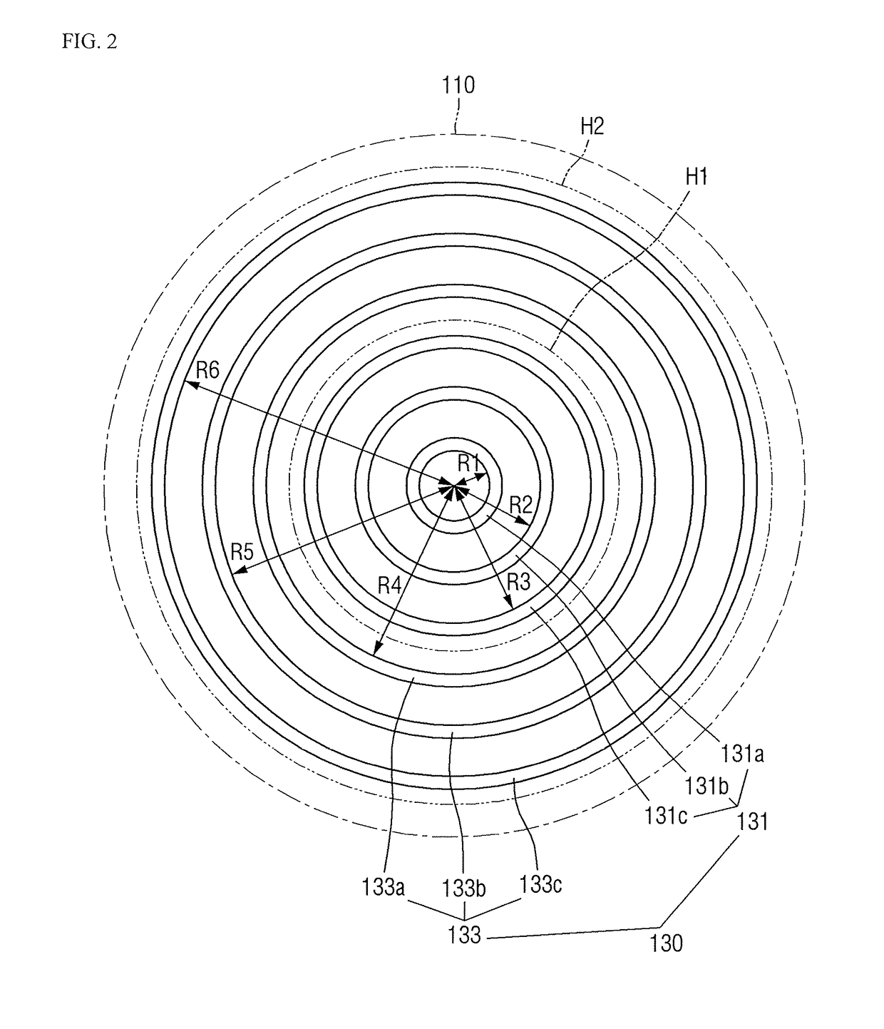
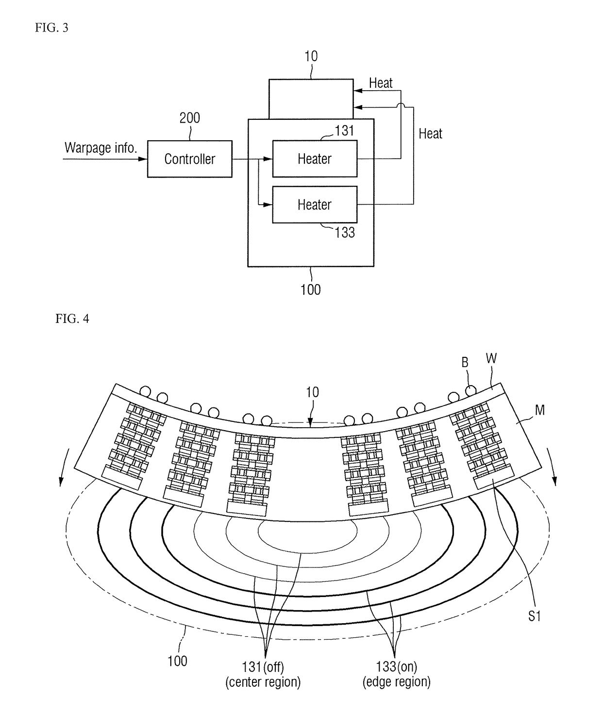
[0027]Referring to FIG. 1, an apparatus for reducing wafer warpage according to an exemplary embodiment of the present inventive concept may include a stage 100.

[0028]The stage 100 may test a mold wafer structure 10. As an example, the mold wafer structure 10 may be disposed on and / ...


PUM


Abstract

An apparatus and a method for reducing wafer warpage are provided. The method includes positioning a mold wafer structure on a stage. The mold wafer structure includes a mold layer and a stack structure positioned on a wafer. The stage includes a center region and an edge region adjacent the center region. Warpage information of the mold wafer structure is obtained. The mold wafer structure is heated by the stage based on the warpage information to reduce a warpage of the mold wafer structure. A temperature of the center region and a temperature of the edge region are different from each other. An operation test is performed on the stack structure.

Description

CROSS-REFERENCE TO RELATED APPLICATION[0001]This application claims priority under 35 USC § 119 to Korean Patent Application No. 10-2016-0117729 filed on Sep. 13, 2016 in the Korean Intellectual Property Office, the disclosure of which is incorporated by reference herein in its entirety.1. TECHNICAL FIELD[0002]Exemplary embodiments of the present inventive concept relate to an apparatus for reducing wafer warpage, and more particularly to a method for reducing wafer warpage.2. DISCUSSION OF RELATED ART[0003]A wafer might not be fixed to equipment during assembly and test processes and thus wafer warpage may occur after a mold process. Wafer warpage may result from a difference in respective thermal expansion coefficients of a film material, a mold material, and a stack structure bonding material of a silicon device.SUMMARY[0004]An exemplary embodiment of the present inventive concept provides an apparatus for reducing wafer warpage.[0005]An exemplary embodiment of the present invent...

Claims


Application Information

Patent Timeline
Patent Type & Authority Patents(United States)
IPC IPC(8): H01L21/84H01L21/66H01L21/324H01L21/67
CPCH01L22/20H01L21/324H01L21/67288H01L21/67259H01L21/67115H01L21/67103H01L21/67248H01L21/6838H01L22/12H01L2224/16145H01L2224/16225H01L2924/181H01L2924/15311H01L2924/3511H01L2924/00012H01L23/562H01L21/565H01L21/6835
Inventor KIM, CHANG HO
Owner SAMSUNG ELECTRONICS CO LTD
Why Eureka
Try Eureka