Electronic product comprising a component having triskelion-pillars, and corresponding fabrication method

a technology of triskelion pillars and electronic components, applied in the field of integration, can solve the problems of poor mechanical robustness of the structure, limited by the etching rate of the process used to form the holes, and high value capacitance will consume a significant area of silicon, so as to reduce the warpage or limit the stress effect of the wafer

Active Publication Date: 2021-02-04
MURATA MFG CO LTD
View PDF0 Cites 2 Cited by
  • Summary
  • Abstract
  • Description
  • Claims
  • Application Information

AI Technical Summary

Benefits of technology

[0025]This arrangement of pillars is very advantageous as regards the surface area of the first electrode. This arrangement is possible because a triskelion arrangement has a substantially triangular shape.
[0026]It has been observed that the arrangement of the pillars in a matrix also participates in reducing wafer warpage or limits stress because the structure of each extends in three directions and comprises bends. This limits the amount of parallel linear trenches aligned in the same direction which may cause significant wafer warpage.

Problems solved by technology

However planar capacitors provide low capacitance density, this implies that a high value capacitance will consume a significant area of silicon.
While this structure is particularly robust (in terms of mechanical robustness), it is also limited by the etching rates of the processes used to form the holes.
The etching rate is consequently improved, but it has been observed that the mechanical robustness of this structure is poor as the pillars may bend prior to the deposition of the dielectric and of the upper electrode.
This generates process issues that can decrease capacitance density, increase the capacitor leakage current and even degrade the breakdown voltage by generating early failures.
It has been observed that greater aspect ratios still lead to bended pillars and too much sticking.

Method used


Image

  • Electronic product comprising a component having triskelion-pillars, and corresponding fabrication method
  • Electronic product comprising a component having triskelion-pillars, and corresponding fabrication method
  • Electronic product comprising a component having triskelion-pillars, and corresponding fabrication method

Examples


Embodiment Construction

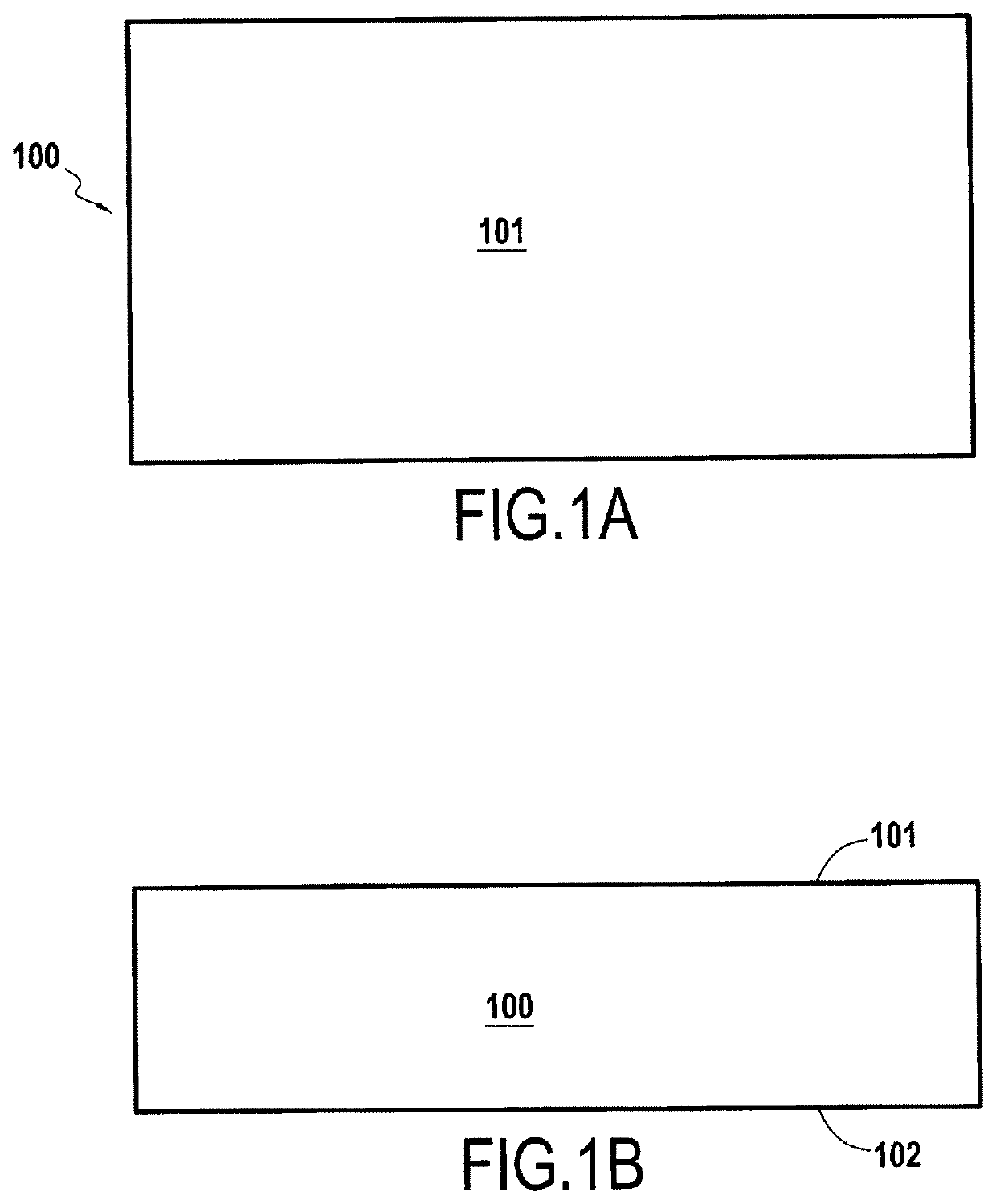
[0046]An electronic product having a first electrode will now be described according to an embodiment. More precisely, the steps for fabricating this electronic product according to an embodiment will be described hereinafter.

[0047]FIG. 1A is a top view of a semi-conductor substrate 100, and in this example the substrate is a silicon substrate, and FIG. 1B is a cross-section view of the substrate 100. The invention is however not limited to silicon substrates and also applies to other types of materials.

[0048]The silicon substrate 100 comprises a top surface 101 and a bottom surface 102 (the wordings top and bottom may of course be interchangeable).

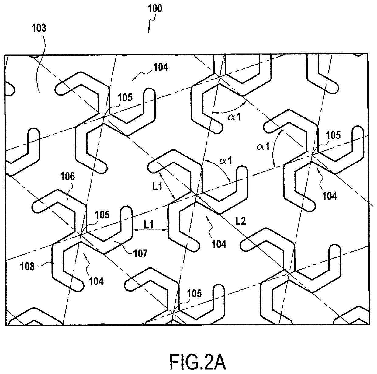
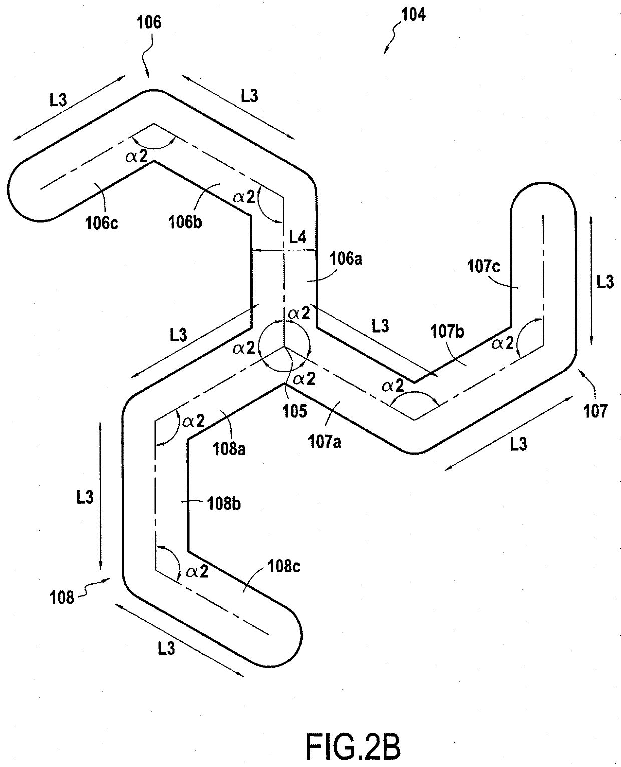
[0049]It is from the top surface 101 that fabrication processes will carried out to form a first electrode. More precisely, a DRIE step may be carried out on the top surface 101 to delimit pillars forming at first electrode, as will be described in reference to FIGS. 2A and 2B.

[0050]FIG. 2A represents a top view of the substrate 100 after...


PUM

PropertyMeasurementUnit
anglesaaaaaaaaaa
aspect ratioaaaaaaaaaa

Abstract

An electronic product that includes a component having a first electrode with a first surface and a pillar extending from the first surface in a first direction, the pillar having three protrusions, the three protrusions forming angles of about 120 degrees with each other around a central line of the pillar where the three protrusions meet, and the three protrusions being bent so that the pillar has a triskelion cross-section in a plane perpendicular to the first direction.

Description

CROSS REFERENCE TO RELATED APPLICATIONS[0001]The present application is a continuation of International application No. PCT / IB2019 / 000294, filed Apr. 26, 2019, which claims priority to European Patent Application No. 18305520.1, filed Apr. 26, 2018, the entire contents of each of which are incorporated herein by reference.FIELD OF THE INVENTION[0002]The present invention relates to the field of integration and, more particularly, to electronic products, related semiconductor products, and their methods of manufacture.[0003]The present invention more precisely relates to electronic components comprising electrodes such as capacitors.TECHNICAL BACKGROUND[0004]Electronic components such as capacitors may be integrated into semiconductor products in a variety of forms. For example, planar capacitors may be formed above semiconductor substrates by forming two planar electrodes separated by a dielectric layer. However planar capacitors provide low capacitance density, this implies that a ...

Claims


Application Information

Patent Timeline
Patent Type & Authority Applications(United States)
IPC IPC(8): H01L49/02
CPCH01L28/87H01L21/3083H01L27/0805H01L28/91H01L29/66181H01L29/94
Inventor BOUVIER, STÉPHANELALLEMAND, FLORENT
Owner MURATA MFG CO LTD
Why Eureka
Try Eureka