

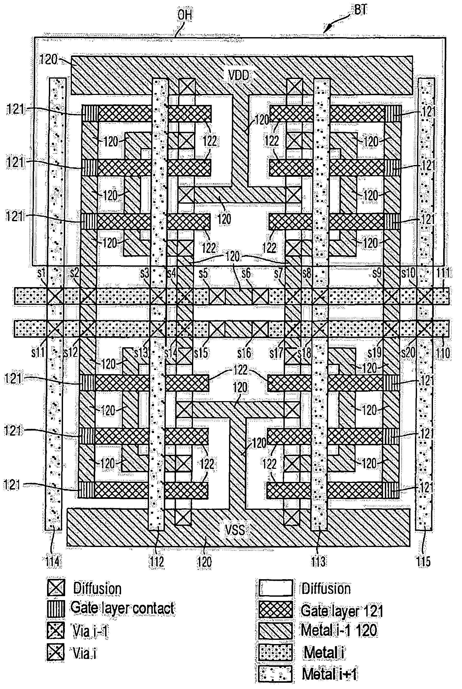
Architecture of function blocks and wirings in a structured ASIC and configurable driver cell of a logic cell zone
a function block and logic cell technology, applied in the direction of logic circuits using elementary logic circuit components, logic circuits using specific components, pulse techniques, etc., can solve the problems of affecting the routing of lines in the intervening wiring layers, the cost of the active structure mask is the principal proportion of the cost of the set of masks, and the fabrication cost of the individual wiring layers. achieve the effect of maintaining locality and improving capacity utilization
- Summary
- Abstract
- Description
- Claims
- Application Information
AI Technical Summary
Benefits of technology
Problems solved by technology
Method used
Image

Examples
Embodiment Construction
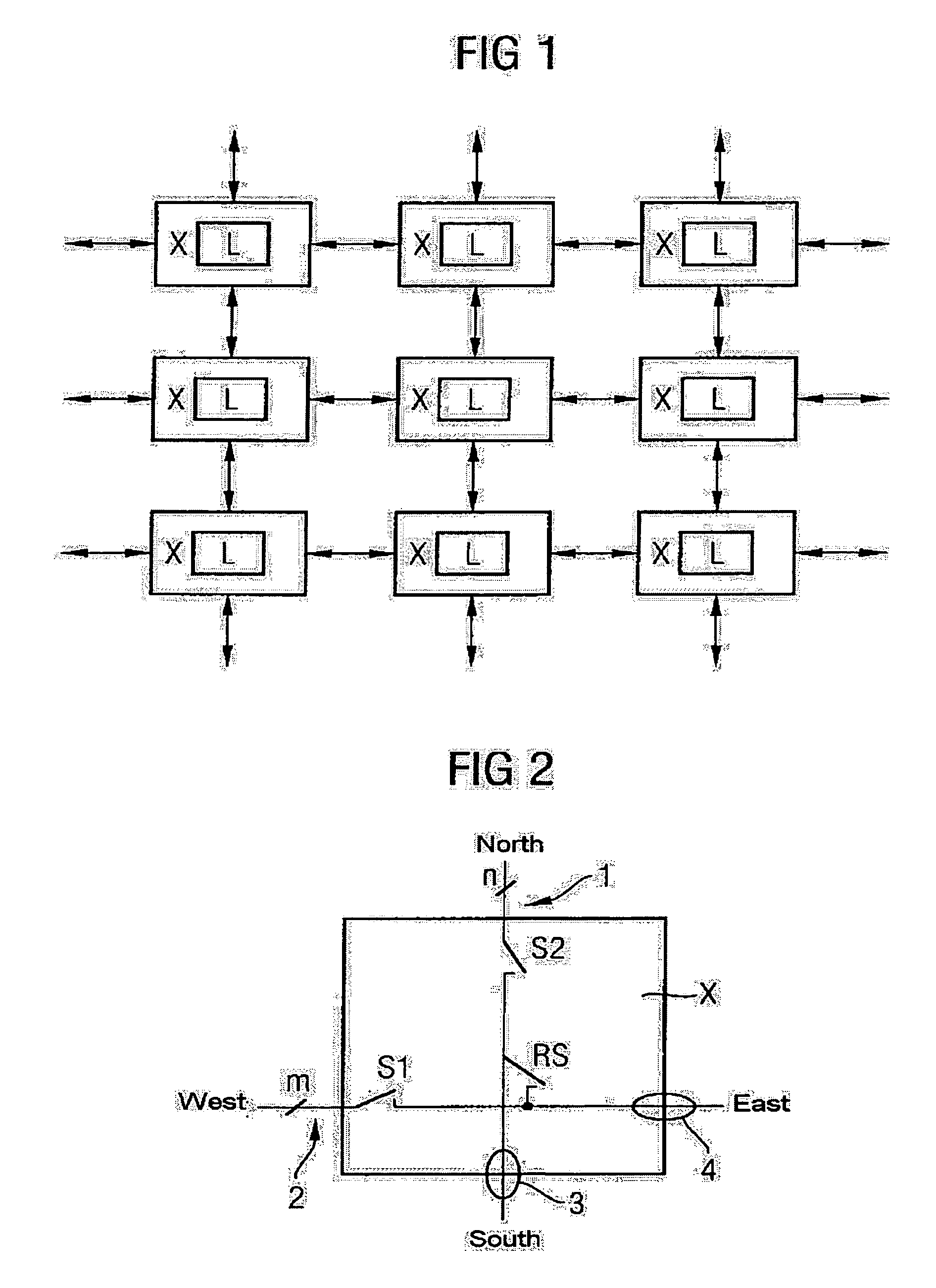
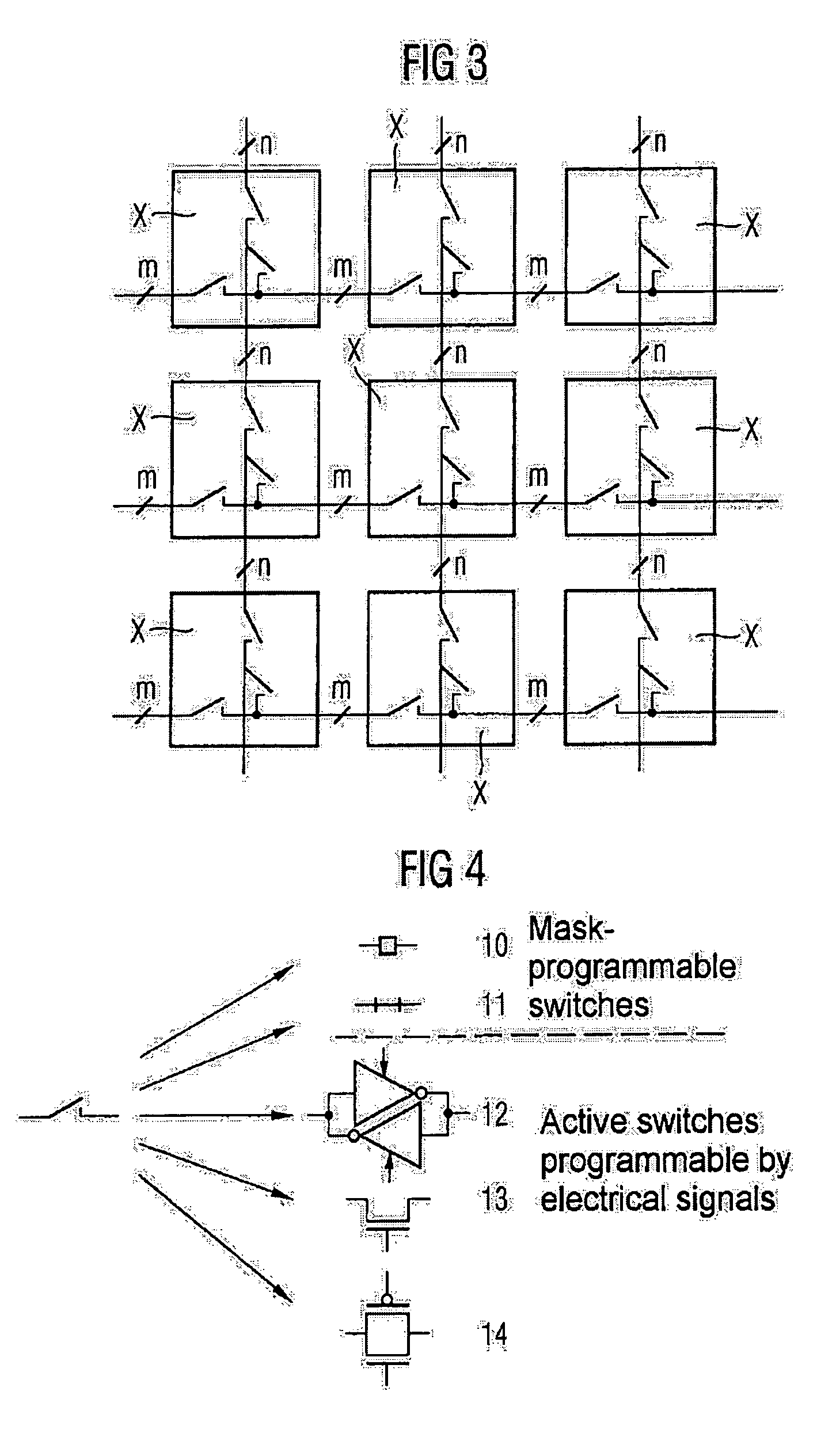
[0064]FIG. 1 schematically shows the architecture of a semiconductor module according to the invention. The semiconductor module is based on an array of logic function blocks L each having identical logic structures. Identical logic structures means that the logic function blocks in the active layer are identical. Each logic function block L is assigned a wiring zone X which contact-connects the respective logic function block with regard to its input and output signals. The wiring zones X are arranged in an array which provides for the routing of the signals between different logic function blocks and corresponds to the array of logic function blocks L. The spacings between the logic function blocks L or the wiring zones X within the arrays are merely illustrated for the sake of better clarity; in practice, the logic function blocks L and the wiring zones X may essentially adjoin one another without any interspaces.
[0065]On account of the geometrical correspondence of the two array...
PUM
 Abstract
Description
Claims
Application Information