Method for producing an electronic module

a technology of electronic modules and vias, applied in the direction of microstructural technology, microstructural devices, electrical apparatus construction details, etc., can solve the problems of cost and pain of producing vias through silicon chips, and achieve the effect of cost-effectiveness

Inactive Publication Date: 2013-08-27
ROBERT BOSCH GMBH
View PDF3 Cites 36 Cited by
  • Summary
  • Abstract
  • Description
  • Claims
  • Application Information

AI Technical Summary

Benefits of technology

[0011]Advantageously, in this way it is possible to avoid vias through a microelectronic component, e.g., a silicon chip, particularly for the contacting of another component. Therefore, within the ambit of the present invention, microelectronic components may be mounted as first and / or second microelectronic components which have no vias. The method of the present invention thus expediently permits cost-effective production of electronic modules, particularly chip-size packages.

Problems solved by technology

However, producing vias through silicon chips is costly and painstaking and includes numerous process steps such as etching, deposition and patterning of insulating layers and metallization.

Method used


Image

  • Method for producing an electronic module
  • Method for producing an electronic module
  • Method for producing an electronic module

Examples


Embodiment Construction

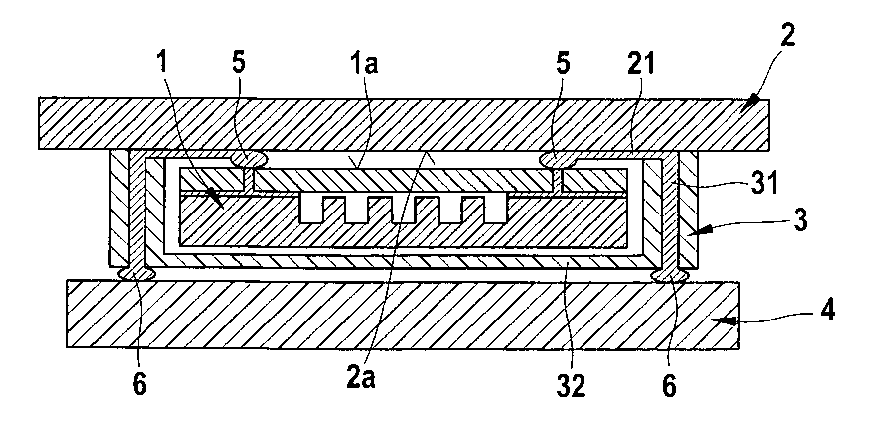
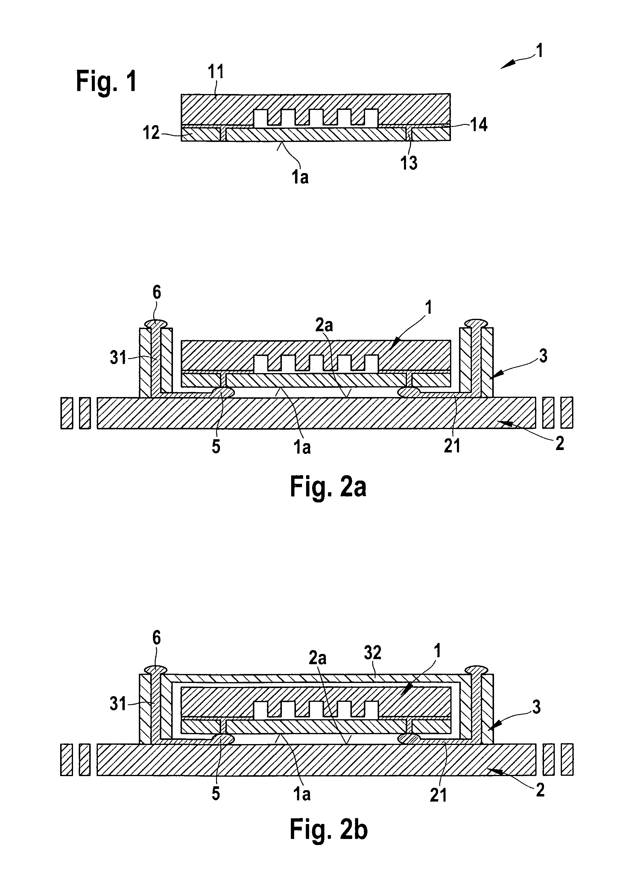
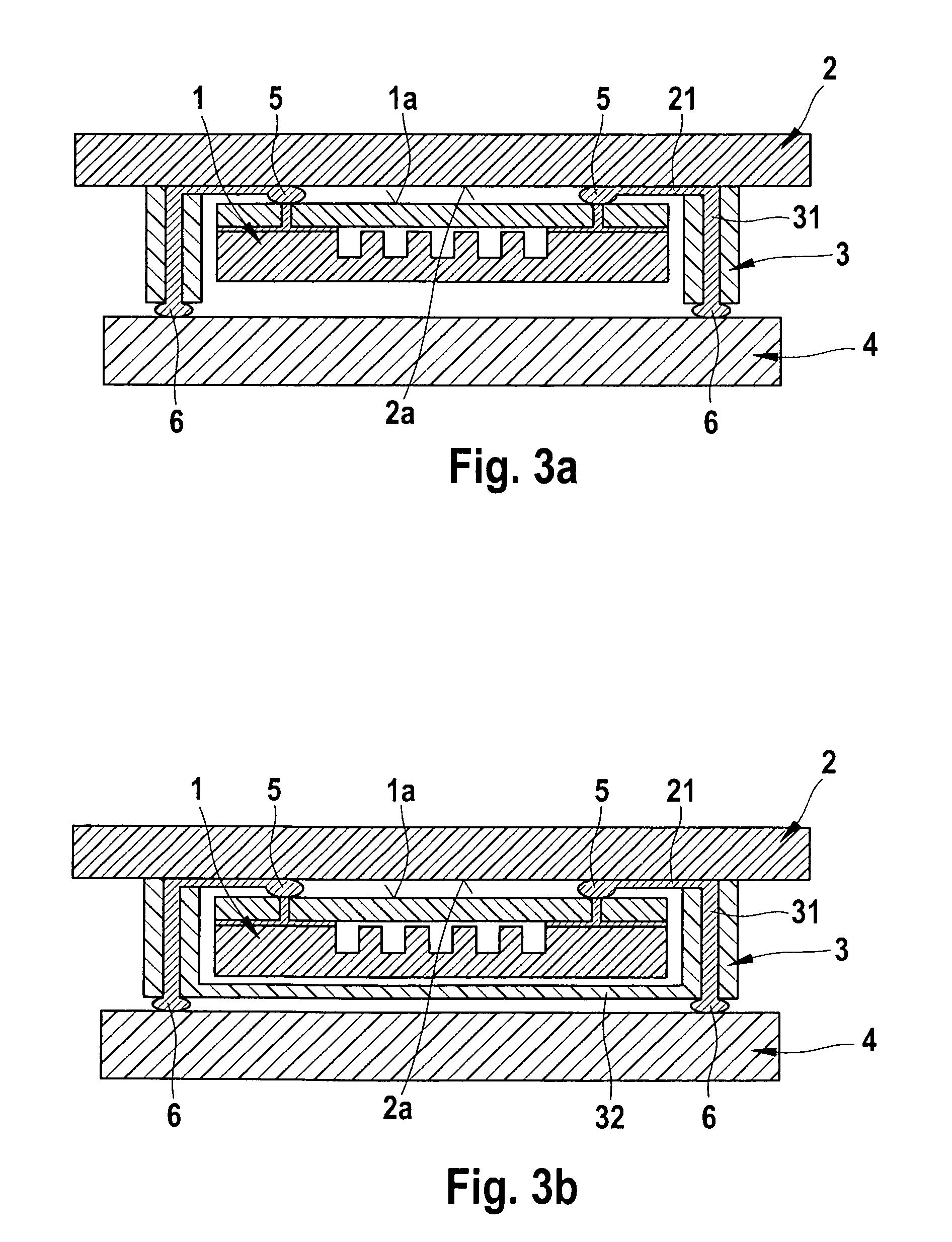
[0017]Within the scope of the present invention, the first and / or the second microelectronic component may be a microchip. In particular, the first and / or the second microelectronic component may in each case have a contacting side. For example, as customary in the flip-chip method, the first and / or the second microelectronic component may in each instance have only one contacting side. Accordingly, the electronic module may have a double flip-chip construction, e.g., an (IC-) flip-chip / (MEMS-) flip-chip hybrid construction.

[0018]Within the scope of the present invention, the first microelectronic component may be electrically connected to the printed circuit board by way of the second microelectronic component and by way of one of the printed circuit traces of the dielectric component.

[0019]Within the context of one specific embodiment of the method according to the present invention, the contacting side of the first microelectronic component is electrically connected to the contac...


PUM

PropertyMeasurementUnit
heightaaaaaaaaaa
dielectricaaaaaaaaaa
thermal expansion coefficientsaaaaaaaaaa

Abstract

A method for producing an electronic module, in that at least one first microelectronic component is provided and is electrically connected to a second microelectronic component by a first flip-chip method step; at least one dielectric component is provided which has at least one printed circuit trace, and at least one printed circuit trace of the dielectric component is electrically connected to the second microelectronic component; and the second microelectronic component is electrically connected by a second flip-chip method step to a printed circuit board by way of the printed circuit trace(s) of the dielectric component, in order to avoid vias through a microelectronic component; the invention also relates to a corresponding electronic module.

Description

BACKGROUND OF THE INVENTION[0001]1. Field of the Invention[0002]The present invention relates to a method for producing an electronic module, as well as an electronic module.[0003]2. Description of Related Art[0004]A multitude of packaging concepts exist for bringing together different sized semiconductor chips, such as microelectromechanical system chips (MEMS chips) and application-specific integrated circuit chips (ASIC chips). They are usually based on ceramic, premold or mold packages, in which the chips are placed side by side or one upon the other, and are connected to each other and to the external contacts by wire bonds.[0005]Microelectromechanical system chips may be mounted on application-specific integrated circuit chips using flip-chip technology. In so doing, the contacting of the microelectromechanical system chip is usually accomplished by way of through-silicon vias (TSV) through the application-specific integrated circuit chip. However, producing vias through silic...

Claims


Application Information

Patent Timeline
Patent Type & Authority Patents(United States)
IPC IPC(8): H05K7/00
CPCB81C1/0023H01L25/0657H01L25/16H01L2225/06513H01L2225/06541Y10T29/49208H01L2924/1433H01L2924/0002H01L2924/14H01L2924/00
Inventor SCHMIDT, MANUELAFRANKE, AXELZINOBER, SVEN
Owner ROBERT BOSCH GMBH
Why Eureka
Try Eureka