Touch screen display and electronic device including same

a touch screen display and electronic device technology, applied in the direction of instruments, other domestic objects, synthetic resin layered products, etc., to achieve the effect of simplifying the stacking process between the electronic device components, reducing weight, and reducing the weight of electronic devices

Active Publication Date: 2021-12-07
SAMSUNG ELECTRONICS CO LTD
View PDF33 Cites 0 Cited by
  • Summary
  • Abstract
  • Description
  • Claims
  • Application Information

AI Technical Summary

Benefits of technology

[0007]According to various embodiments, a structural improvement of the touch screen display may realize miniaturization, weight-saving, or flexibility of the electronic device.
[0008]According to various embodiments, the stacking process between the electronic device components may be simplified.
[0009]In addition to this, various effects may be provided that are directly or indirectly grasped through the disclosure.

Problems solved by technology

Miniaturizing, weight-saving, or improving portability of the electric device are on the rise of a major issue of the development.

Method used


Image

  • Touch screen display and electronic device including same
  • Touch screen display and electronic device including same
  • Touch screen display and electronic device including same

Examples


first embodiment

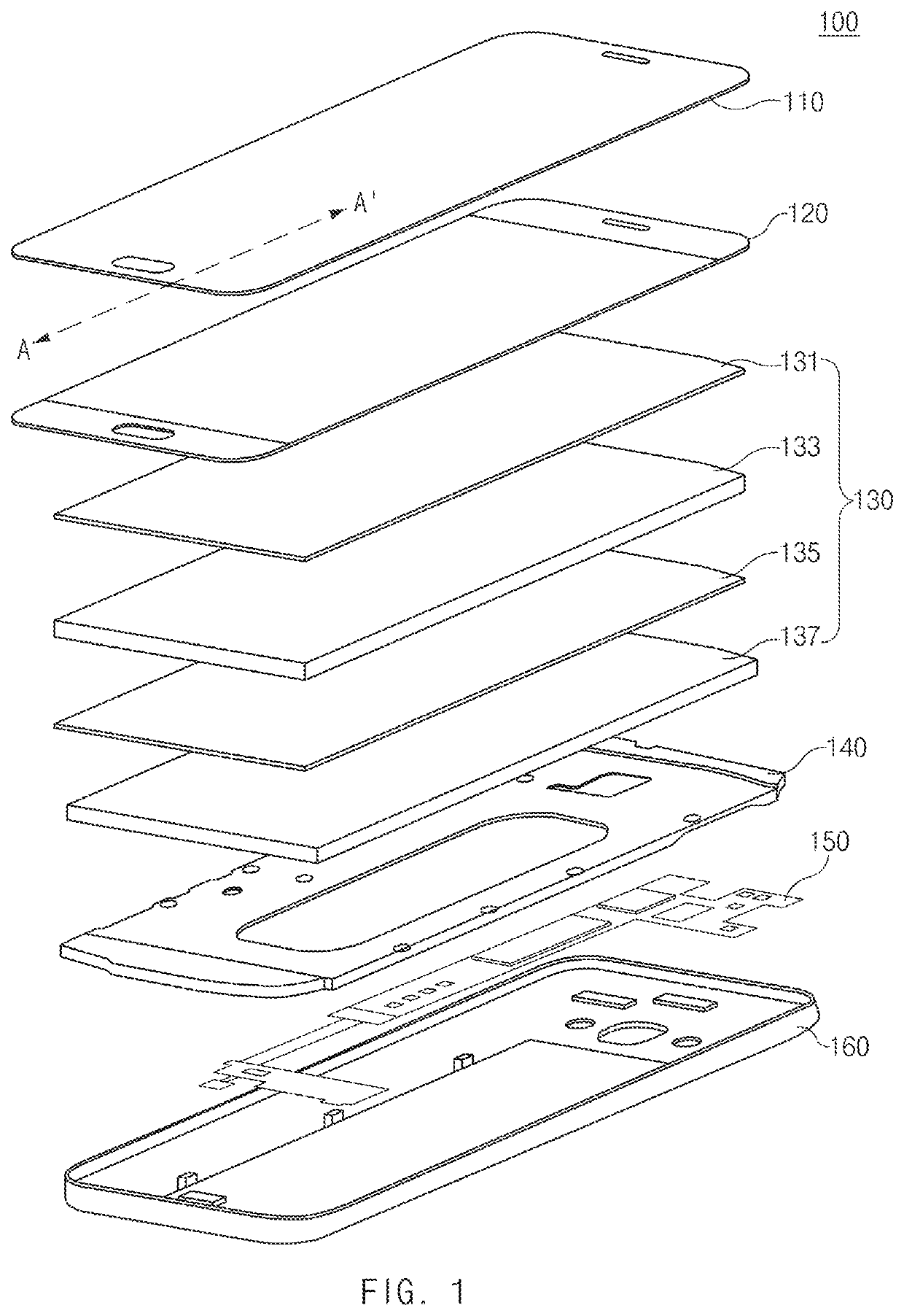
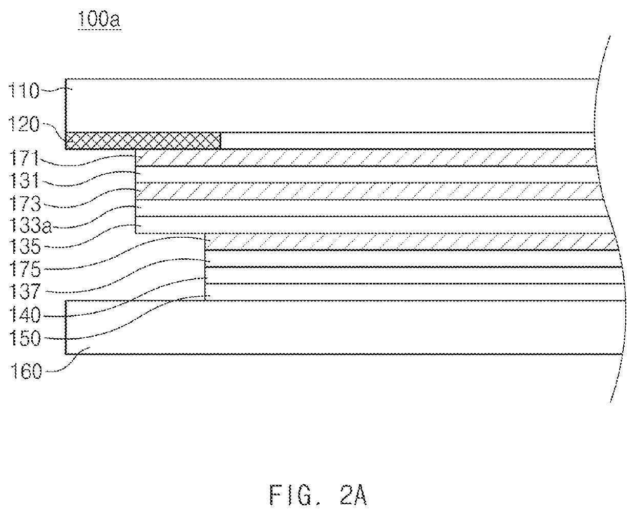
[0050]With reference to FIG. 2A, at least some of components of an electronic device 100a may be stacked in a predetermined order in a first direction (e.g., upper direction side of the support member 140) on the support member 140. For example, the display panel 137, the second polarizing plate 135, a touch panel 133a, the first polarizing plate 131, the cover glass 110 to which the printed member 120 is adhered, and the like may be stacked in order on the top surface of the support member 140.

[0051]With respect to the stacked structure between the components, the photosensitive adhesive member as described above such as photosensitive adhesive members 171, 173, and 175 may be disposed in at least some of spaces between the components. For example, the third photosensitive adhesive member 175, the second photosensitive adhesive member 173, and the first photosensitive adhesive member 171 may be respectively disposed between the display panel 137 and the second polarizing plate 135...

second embodiment

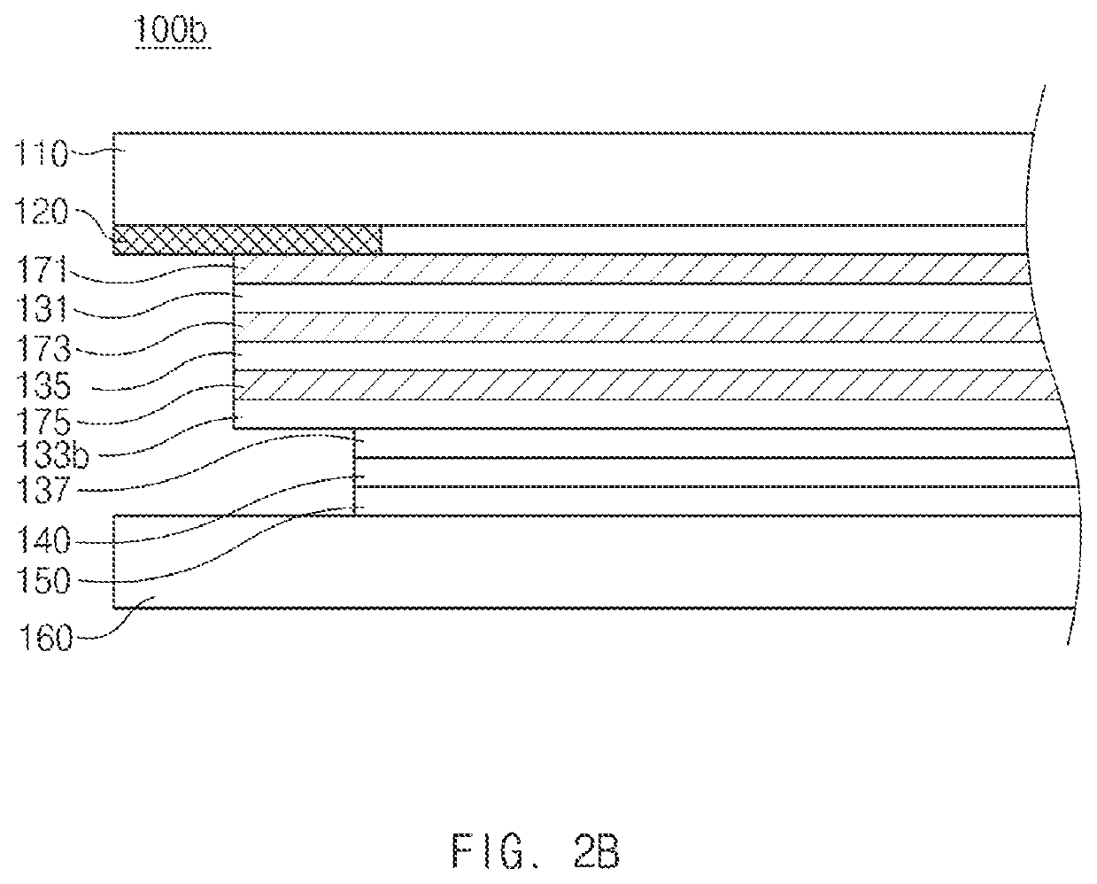
[0057]On the stacked structure of the electronic device 100b the touch panel 133b may be stacked on a top surface of the display panel 137. In this regard, at least some of electrode layers included in the touch panel 133b may be included in the display panel 137. For example, a first electrode layer (e.g., Rx electrode layer) of the touch panel 133b may be mounted on an upper substrate constituting the display panel 137 or formed on the upper substrate (e.g., on-cell mode). Alternatively, the first electrode layer (e.g., Rx electrode layer) and a second electrode layer (e.g., Tx electrode layer) of the touch panel 133b may be formed within the display panel 137 (e.g., in-cell mode). In a case of the in-cell mode, a substrate forming the electrode layer of the touch panel 133b may be excluded, which may contribute to miniaturizing or weight-saving of the electronic device 100b.

[0058]FIGS. 3A to 3C are diagrams illustrating stacking processes between at least some components of an ...


PUM

PropertyMeasurementUnit
thicknessaaaaaaaaaa
photosensitiveaaaaaaaaaa
flexibilityaaaaaaaaaa

Abstract

One embodiment of the disclosure discloses a touch screen display including a first polarizing plate, a second polarizing plate disposed under the first polarizing plate, a touch panel disposed between the first polarizing plate and the second polarizing plate, a display panel disposed under the second polarizing plate, and a photosensitive adhesive member disposed at least between the first polarizing plate and the touch panel or between the second polarizing plate and the display panel. Further, one embodiment of the disclosure discloses an electronic device including the touch screen display. In addition, various embodiments are possible which are understood through the specification.

Description

PRIORITY[0001]This application is a National Phase Entry of PCT International Application No. PCT / KR2017 / 010984 which was filed on Sep. 29, 2017, and claims priority to Korean Patent Application No. 10-2016-0129855, which was filed on Oct. 7, 2016, the content of each of which is incorporated herein by reference.TECHNICAL FIELD[0002]Embodiments disclosed herein relate to a stacked structure of a touch screen display.BACKGROUND ART[0003]Recently, as an electronic device equipped with a proprietary operating system is spread rapidly, an electronic device supports various functions such as internet service, digital broadcast viewing, a mobile game, or the like in addition to a call function. As such, the electronic device evolved into a multifunctional medium is becoming a daily necessity for modern people who are living in a ubiquitous society. Accordingly, the electronic device is being developed in a way to minimize limitations of the operating environment. Miniaturizing, weight-sav...

Claims


Application Information

Patent Timeline
Patent Type & Authority Patents(United States)
IPC IPC(8): B32B17/06B32B7/02B32B7/14B32B7/12
CPCB32B17/06B32B7/02B32B7/12B32B7/14B32B17/10B32B27/08B32B2457/208B32B2457/206G06F1/1626G06F1/1643H04M1/0266G06F2203/04103G06F3/0412G06F2203/04102B32B2457/202
Inventor KIM, MIN UK
Owner SAMSUNG ELECTRONICS CO LTD
Why Eureka
Try Eureka