Eureka AIR delivers breakthrough ideas for toughest innovation challenges, trusted by R&D personnel around the world.

Optical module

a technology of optical modules and optical components, applied in the direction of high frequency circuit adaptations, electrical apparatus construction details, printed circuit non-printed electric components association, etc., can solve problems such as deterioration of frequency characteristics of optical modules, and achieve the effect of preventing deterioration of frequency characteristics

Active Publication Date: 2022-04-26
CIG PHOTONICS JAPAN LTD
View PDF12 Cites 0 Cited by
  • Summary
  • Abstract
  • Description
  • Claims
  • Application Information

AI Technical Summary

Benefits of technology

[0007]This enables the ground pad to be close to the signal-line portion, thereby preventing deterioration of the frequency characteristics.

Problems solved by technology

Alternatively, with the pads being thinner, workability of soldering worsens, leading to uneven bonding, posing a problem of deterioration in frequency characteristics of the optical module.

Method used


Image

  • Optical module
  • Optical module
  • Optical module

Examples


first embodiment

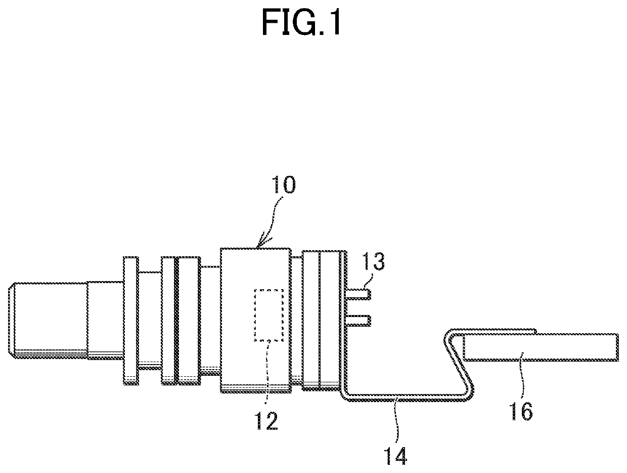
[0026]FIG. 1 is a perspective view of an optical module according to a first embodiment. The optical module is a TO-CAN (Transistor Outline-Can) type optical module and has an optical subassembly 10. The optical subassembly 10 may be any of an optical transmission subassembly with a light emitting device (TOSA: Transmitter Optical Sub-Assembly), an optical reception subassembly with a light receiving device (ROSA: Receiver Optical Sub-Assembly), and a two-way module with both a light emitting device and a light receiving device (BOSA: Bidirectional Optical Sub-Assembly). The optical sub-assembly 10 includes a photoelectric device 12 for converting the optical signal and the electrical signal at least from one to another. The optical subassembly 10 has lead pins 13 for electrical connection between the photoelectric device 12 and the outside. A flexible printed circuit board (FPC) 14 is connected to the lead pins 13. The flexible printed circuit board 14 is connected to a printed cir...

second embodiment

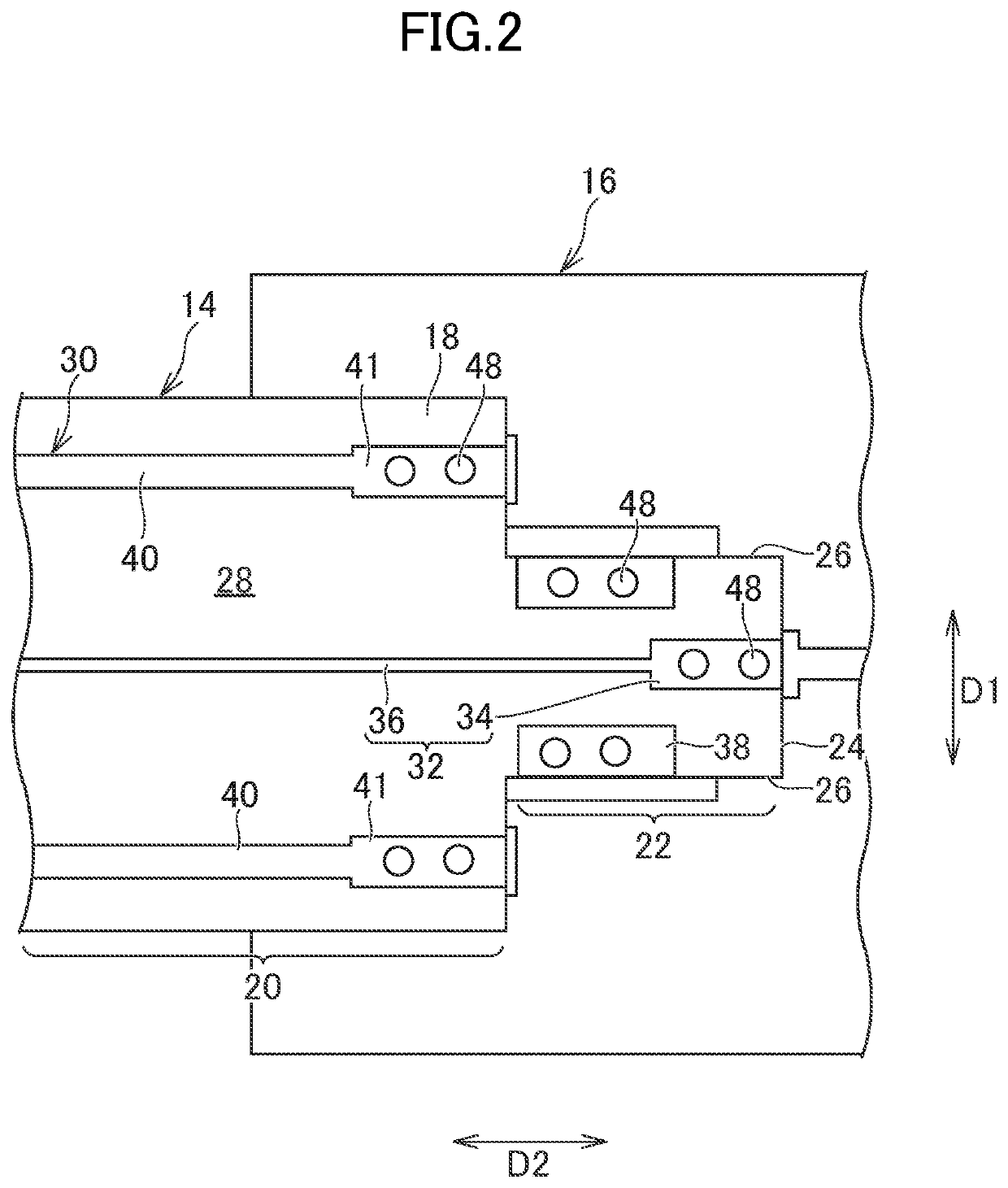
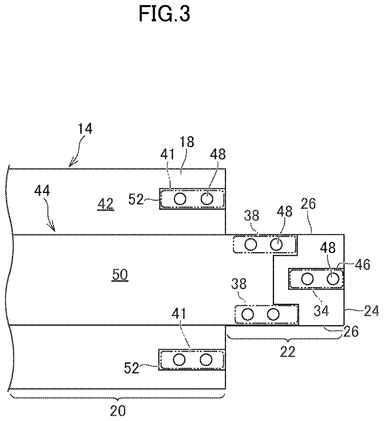
[0041]FIG. 7 is a plan view of a first surface of a flexible printed circuit board in a second embodiment. FIG. 8 is a plan view of a second surface of the flexible printed circuit board in the second embodiment. The insulating substrate 218 has some projections 222, and a slit 264 between the adjacent projections 222. This reduces the heat capacity of the flexible printed circuit board 214 (insulating substrate 218), even improves the visibility of the connection portion by the conductive connecting material 62, and improves the robustness as well. On the first surface 228, the first wiring pattern 230 includes some pairs (e.g., four pairs) of ground pads 238 and includes some signal wires 232. On the second surface 242, the second wiring pattern 244 includes some signal pads 246. The pitch between adjacent signal pads 246 is 1.5 mm or more. The contents described in the first embodiment are applicable to the present embodiment.

[0042]FIG. 9 is a diagram of frequency characteristics...


PUM

PropertyMeasurementUnit
distanceaaaaaaaaaa
flexibleaaaaaaaaaa
shapeaaaaaaaaaa

Abstract

An optical module includes a photoelectric device and a flexible printed circuit board. The flexible printed circuit board includes an insulating substrate with a first surface and a second surface, a first wiring pattern on the first surface, and a second wiring pattern on the second surface. The first wiring pattern includes a signal line with a signal terminal portion at a tip and a signal-line portion narrower than the signal terminal portion, the first wiring pattern including a pair of ground pads at positions sandwiching the signal-line portion, at least part of the pair of ground pads avoiding being adjacent to the signal terminal portion. The second wiring pattern includes a ground plane overlapping with the signal-line portion and being connected to the pair of ground pads, the second wiring pattern including a signal pad connected to the signal terminal portion.

Description

CROSS-REFERENCE TO RELATED APPLICATION[0001]The present application claims priority from Japanese patent application JP2019-230383 filed on Dec. 20, 2019, the contents of which are hereby incorporated by reference into this application.BACKGROUND1. Field[0002]This relates to an optical module.2. Description of the Related Art[0003]A flexible printed circuit board (FPC) in an optical module has pads arranged in a horizontal row for electrical connection with the outside (JP 2016-51770A, JP 2004-247980A). For example, a pad for transmitting high frequency signals is in a position sandwiched between other pads for being connected to a ground pattern.[0004]With the pads arranged in a horizontal row, the flexible printed circuit board is wider. Alternatively, with the pads being thinner, workability of soldering worsens, leading to uneven bonding, posing a problem of deterioration in frequency characteristics of the optical module. SUMMARY[0005]This aims at preventing deterioration of f...

Claims


Application Information

Patent Timeline
Patent Type & Authority Patents(United States)
IPC IPC(8): H05K7/00H05K1/14H05K1/11H05K1/18H05K3/28
CPCH05K1/147H05K1/113H05K1/118H05K1/189H05K3/28H05K2201/10121H01L31/0203H01L31/02005H01L31/02002H05K1/117H05K1/0219H05K1/0253H05K2201/09427
Inventor NOGUCHI, DAISUKEYAMAMOTO, HIROSHI
Owner CIG PHOTONICS JAPAN LTD
Why Eureka
Eureka Blog
Learn More