Display panel and electronic device

a technology of electronic devices and display panels, applied in the field of display technology, can solve the problems of panel to display horizontal, extreme sensitivity to impedance differences between ck (clock) signals of goa circuits, and heavy loading of 8k ultra-high resolution electronic devices

Active Publication Date: 2022-10-04
SHENZHEN CHINA STAR OPTOELECTRONICS SEMICON DISPLAY TECH CO LTD
View PDF39 Cites 3 Cited by
  • Summary
  • Abstract
  • Description
  • Claims
  • Application Information

AI Technical Summary

Benefits of technology

[0005]The present disclosure provides a display panel and an electronic device to alleviate the technical problem of a difference of the output signal of the GOA unit caused by a CK impedance difference existing in the currently 8K ultra-high resolution electronic device.
[0051]Beneficial effect of the present disclosure: The present disclosure provides a display panel and an electronic device, the display panel comprising m GOA units arranged in a column direction, each of the GOA units comprises a pull-up module, the pull-up module comprises a clock input transistor connected to a clock signal; n clock signal lines extending in the column direction and arranged in parallel; and m clock signal connection lines extending in a row direction and arranged in parallel, the m clock signal connection lines corresponding one-to-one with the m GOA unit, configured to connect the clock input transistor of the pull-up module of the GOA unit to the corresponding clock signal line; wherein the n clock signal lines comprise n1st clock signal line and n2nd clock signal line, the n2nd clock signal line is formed on a side away from the GOA unit of the n1st clock signal line, a voltage drop value of the clock input transistor of pull-up module of m1st GOA unit connected to the n1st clock signal line is greater than a voltage drop value of the clock input transistor of pull-up module of m2nd GOA unit connected to the n2nd clock signal line. Based on this circuit structure, by adjusting the voltage drop values of the clock input transistors of different GOA units, the voltage drop values caused by the different lengths of the clock signal line and the clock signal connection line can be compensated. Thereby making the voltage drop value between each GOA unit and the clock driving chip are approximately the same, alleviating the CK impedance difference existing in 8K ultra-high resolution electronic device and improves the technical problems of 8K ultra-high resolution electronic devices that lead by the difference in the output signal of the GOA unit.

Problems solved by technology

For example, 8K ultra-high resolution electronic devices have heavy loading (short voltage drop) and short charging time.
Due to adoption of GOA circuits (Gate on Array, gate drive circuit integrated on the array substrate) and a thick copper design, this results in an extreme sensitivity to impedance differences between CK (clock) signals of ultra-high resolution electronic devices and the GOA circuits.
As a result, there is a difference between the CK pattern and the scan line waveform output by the corresponding GOA unit, causing the panel to display horizontal lines and othe similar problems.
Therefore, current 8K ultra-high resolution electronic devices have at least a technical problem in that the difference in the CK impedance causes a difference between the output signals of each GOA unit, which needs to be improved.

Method used


Image

  • Display panel and electronic device
  • Display panel and electronic device
  • Display panel and electronic device

Examples


Embodiment Construction

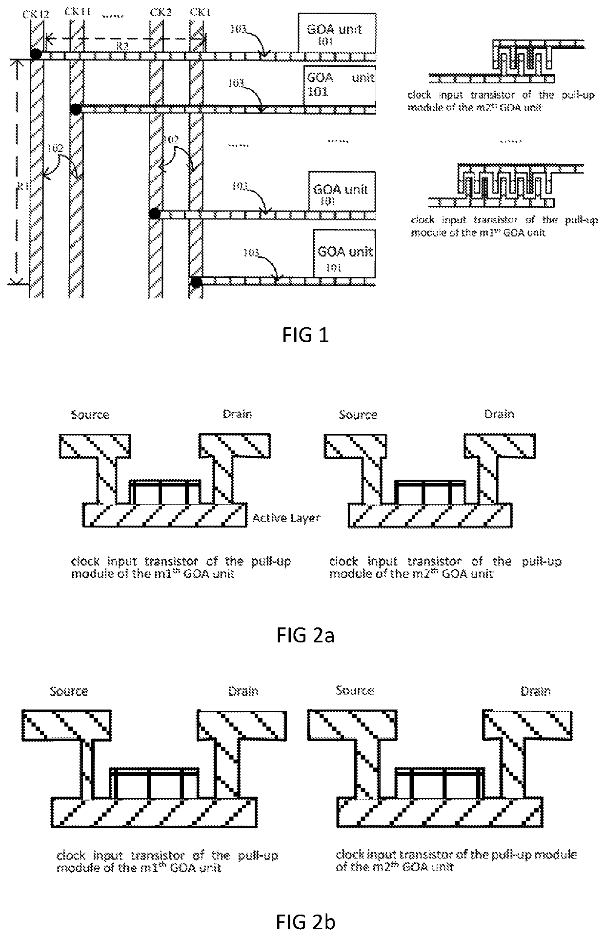
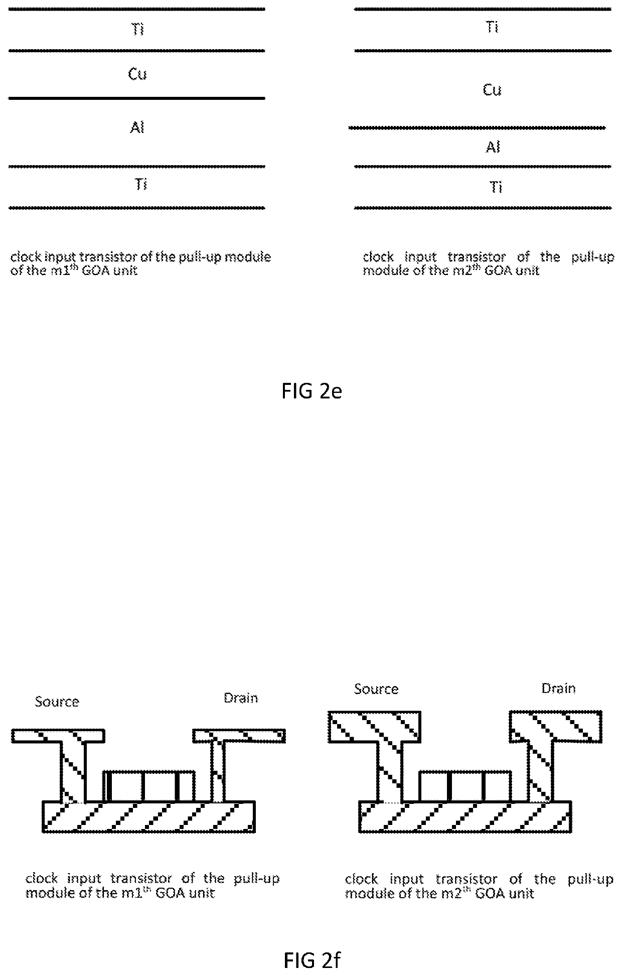
[0062]The following is a description of each embodiment with reference to additional figures to illustrate specific embodiments in which the present disclosure can be implemented. The directional terms mentioned in the present disclosure, such as up, down, front, back, left, right, inside, outside, side, etc., are only directions referring to the figures. Therefore, the directional terms are to explain and understand the disclosure, not to limit it. In the figure, similarly structured units are denoted by the same reference numerals.

[0063]In the following, the technical solutions in the embodiments of the present disclosure will be clearly and completely described with reference to the figures. Obviously, the described embodiments are only some embodiments of the present disclosure, not all the embodiments. Based on the embodiments in the present disclosure, all other embodiments obtained by a person of ordinary skill in the art without creative steps shall fall within the protectio...


PUM


Abstract

A display panel and an electronic device is provided. A voltage drop value of the clock input transistor of a pull-up module of m1st GOA unit connected to an n1st clock signal line is greater than a voltage drop value of the clock input transistor of a pull-up module of m2nd GOA unit connected to the n2nd clock signal line. Based on this circuit structure, a CK impedance difference existing in 8K ultra-high resolution electronic devices can be alleviated.

Description

FIELD OF INVENTION[0001]The present disclosure relates to the field of display technology, and more particularly, to a display panel and an electronic device.BACKGROUND OF INVENTION[0002]With the developments in display technology, the resolution of electronic devices such as display screens, TVs, and mobile phones have become higher and higher, with an increase in resolution corresponding to an increase in the number of pixels, which accompanies a plurality of technical challenges.[0003]For example, 8K ultra-high resolution electronic devices have heavy loading (short voltage drop) and short charging time. Due to adoption of GOA circuits (Gate on Array, gate drive circuit integrated on the array substrate) and a thick copper design, this results in an extreme sensitivity to impedance differences between CK (clock) signals of ultra-high resolution electronic devices and the GOA circuits. The resolution of an 8K electronic device is 7680*4320, there are a total of 4320 rows of GOA un...

Claims


Application Information

Patent Timeline
Patent Type & Authority Patents(United States)
IPC IPC(8): G09G3/3266G09G3/20
CPCG09G3/2092G09G2310/0267G09G3/20G09G3/3677G09G2300/0408G09G2300/0426
Inventor GAO, YANANKIM, LIGONZHAO, BINZHANG, XINZHAO, JUN
Owner SHENZHEN CHINA STAR OPTOELECTRONICS SEMICON DISPLAY TECH CO LTD
Why Eureka
Try Eureka