MOS semiconductor device and method of manufacturing the same

a semiconductor device and semiconductor technology, applied in the direction of microstructural devices, microstructured devices, transistors, etc., can solve the problems of low control capabilities of the gate electrode 94 for the channel region 95, and limited step of the upper surface of the gate electrode to an optimal rang

Inactive Publication Date: 2002-01-10
MITSUBISHI ELECTRIC CORP
View PDF0 Cites 59 Cited by
  • Summary
  • Abstract
  • Description
  • Claims
  • Application Information

AI Technical Summary

Problems solved by technology

Therefore, there is a problem in that control capabilities of the gate electrode 94 for the channel region 95 are low.
In addition, the step of the upper surface of the gate electrode is limited to an optimal range.
Therefore, there is a problem in that it is hard to make a patterning dimension uniform if a height of a film to be patterned is not uniform.
In the thermal oxidation, however, a growth speed of the oxide film has anisotropy because of a crystal surface orientation in the surface of the silicon substrate.

Method used


Image

  • MOS semiconductor device and method of manufacturing the same
  • MOS semiconductor device and method of manufacturing the same
  • MOS semiconductor device and method of manufacturing the same

Examples


fifth embodiment

[0144] Fifth Embodiment

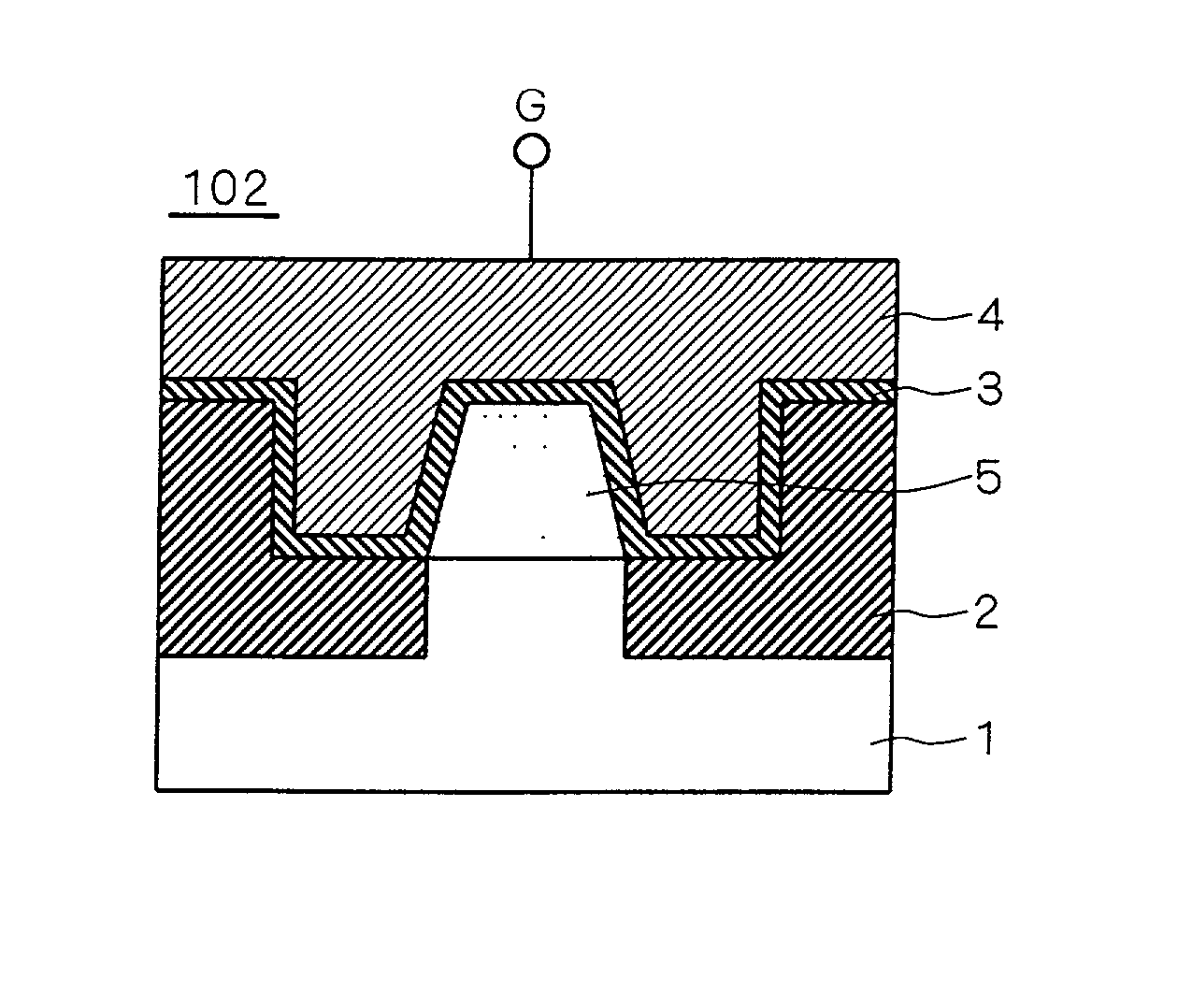
[0145] FIG. 37 is a sectional view showing a MOS semiconductor device according to a fifth embodiment. In the device 108, a gate electrode 4 is opposed to a part of a bottom surface of a channel region 5 as well as an upper surface and side surfaces thereof with a gate insulating film 3 interposed therebetween. Consequently, a charge share ratio of the gate electrode 4 is further increased. Therefore, a short channel effect for a threshold voltage can further be suppressed. Moreover, since an effective channel width is increased, a high current driving capability can be obtained.

[0146] Although the whole channel region 5 can be covered by the gate electrode 4 (which will be presented in a seventh embodiment), it would cause the channel region 5 to temporality float in the air in a manufacturing process and thereby arise a possible strength problem. In this respect, the channel region 5 is always coupled to an insulating layer 21 in the configuration shown in F...

sixth embodiment

[0148] Sixth Embodiment

[0149] The Damascene gate method has recently been proposed as a method of manufacturing a gate electrode of a MOS transistor. The gate electrode 4 covering the channel region 5 can be formed in self-alignment by a combination of the present invention with the Damascene technique. In the present embodiment, such a manufacturing method will be described with reference to the steps shown in FIGS. 39 to 46.

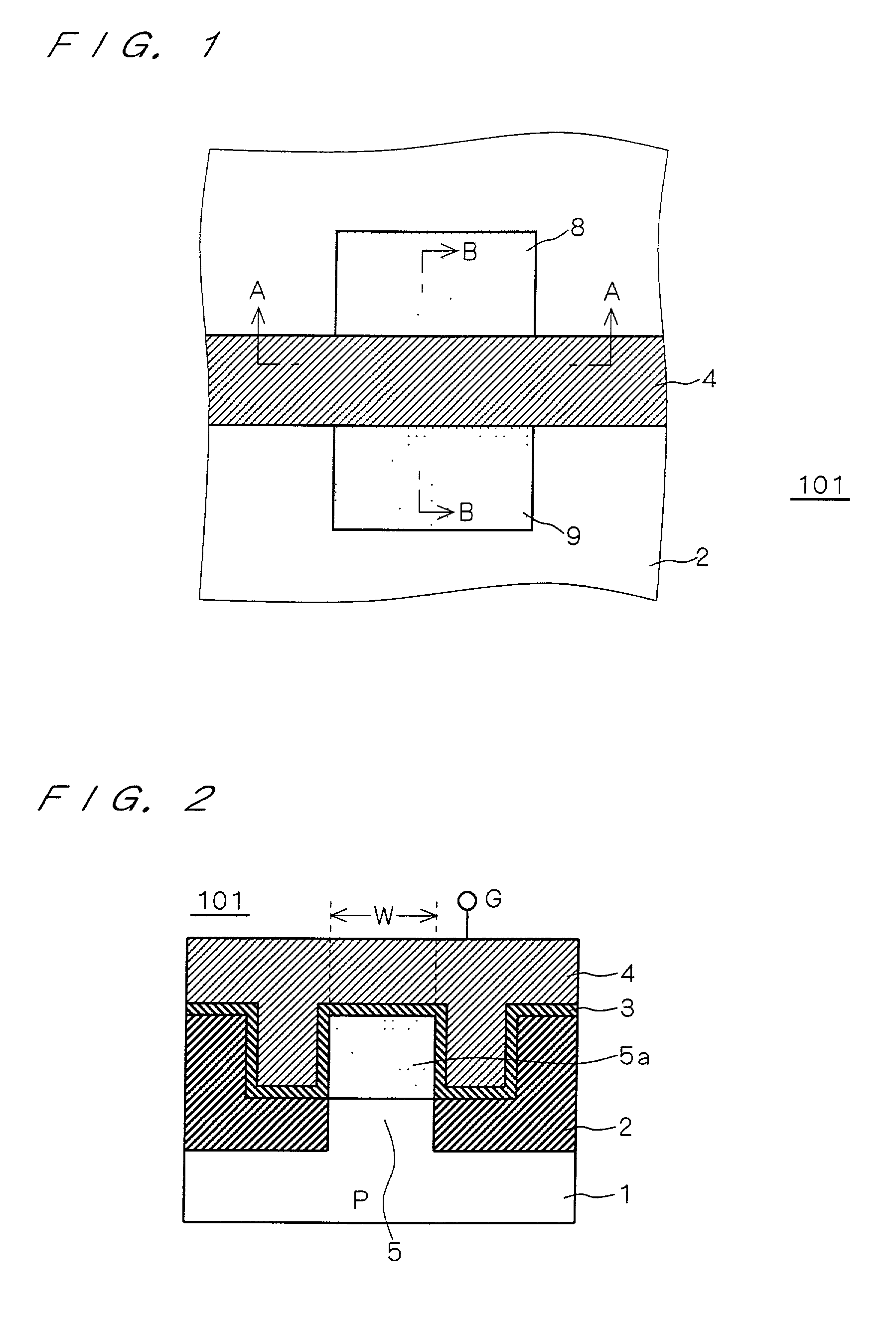
[0150] In the manufacturing method, first of all, a substrate oxide film 6 and a mask nitride film 7 are removed after the steps of FIGS. 6 to 10 are executed. Then, the steps of FIGS. 39 and 40 are executed. FIGS. 39 and 40 are sectional views showing an intermediate structure obtained in the middle of the manufacturing steps, which are taken along the lines B-B and A-A of FIG. 1.

[0151] At the steps of FIGS. 39 and 40, first of all, a silicon oxide film as a sacrificial layer 31 having a thickness of approximately 200 nm is deposited over the whole surface of ...

seventh embodiment

[0158] Seventh Embodiment

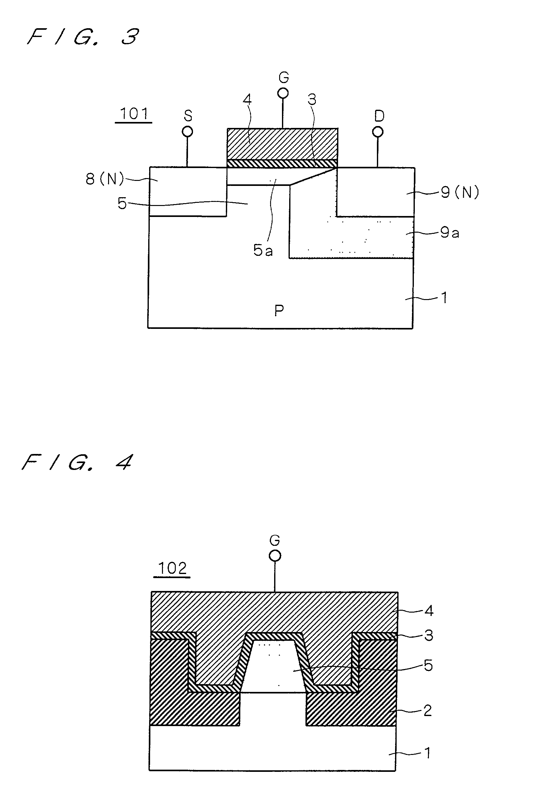
[0159] FIGS. 47 and 48 are sectional views showing a MOS semiconductor device according to a seventh embodiment. FIGS. 47 and 48 correspond to sectional views taken along the lines A-A and B-B when FIG. 1 is seen as a plan view showing the device according to the present embodiment, respectively. In a device 109, a channel region 5 floats above a receding main surface of an SOI substrate and all upper, side and bottom surfaces of the channel region 5 are covered by a gate electrode 4 with a gate insulating film 3 interposed therebetween. Consequently, a charge share ratio of the gate electrode 4 is further increased. Thus, it is possible to further suppress a short channel effect on a threshold voltage. Moreover, since an effective channel width is increased, a high current driving capability can be obtained.

[0160] In order to manufacture the device 109, it is preferable that a so-called gate all around structure should be implemented by utilizing the manufa...


PUM


Abstract

The object of the present invention is to suppress a short channel effect on a threshold voltage. A channel region 5, a pair of source-drain regions and an isolating film 2 having a trench isolation structure are selectively formed in a main surface of a semiconductor substrate 1. An upper surface of the isolating film 2 recedes to be lower than an upper surface of the channel region 5 in a trench portion adjacent to side surfaces of the channel region 5 and to be almost on a level with the upper surface of the channel region 5 in other regions. Consequently, a part of the side surfaces of the channel region 5 as well as the upper surface thereof are covered by a gate electrode 4 with a gate insulating film 3 interposed therebetween. A channel width W of the channel region 5 is set to have a value which is equal to or smaller than a double of a maximum channel depletion layer width Xdm. Moreover, a width of the trench adjacent to the side surfaces of the channel region 5 is set to be equal to or smaller than a double of a thickness of the gate electrode 4.

Description

[0001] 1. Field of the Invention[0002] The present invention relates to a MOS semiconductor device, that is, a semiconductor device having a MOS structure and a method of manufacturing the semiconductor device, and more particularly to an improvement in suppression of a short channel effect of a threshold voltage.[0003] 2. Description of the Background Art[0004] First of all, names to be used in this specification will be described. In this specification, a general semiconductor device comprising a structure including a channel region, a pair of source-drain regions interposing the channel region therebetween and a gate electrode opposed to the channel region with an insulating film interposed therebetween, that is, a MOS structure will be hereinafter referred to as a MOS semiconductor device. Typical examples include a MOS transistor, whereas the MOS semiconductor device is not restricted to the MOS transistor. Although a set of a source region and a drain region which interpose a ...

Claims


Application Information

Patent Timeline
Patent Type & Authority Applications(United States)
IPC IPC(8): H01L21/76H01L21/336H01L21/762H01L29/423H01L29/78H01L29/786
CPCH01L29/42384H01L29/42392H01L29/66795H01L29/785H01L29/7851H01L29/7853H01L29/7854H01L29/78654H01L29/78
Inventor MAEGAWA, SHIGETO
Owner MITSUBISHI ELECTRIC CORP
Why Eureka
Try Eureka