Organic electroluminescent display device

a display device and organic technology, applied in the direction of electroluminescent light sources, static indicating devices, instruments, etc., can solve the problems of reducing space efficiency, difficult arrangement of wirings, and disordered wirings of conventional organic electroluminescent display devices, so as to reduce the degree of accumulation of charges on edge parts, increase the arrangement efficiency of wirings and metal patterns, and relieve the effect of the degree of accumulation of charges

Active Publication Date: 2005-04-14
SAMSUNG DISPLAY CO LTD
View PDF2 Cites 18 Cited by
  • Summary
  • Abstract
  • Description
  • Claims
  • Application Information

AI Technical Summary

Benefits of technology

[0016] Therefore, in order to solve the foregoing problems in the conventional organic electroluminescent display device, in exemplary embodiments of the present invention, charges between adjacent wirings are substantially uniformly distributed in an organic electroluminescent display device by generally rounding the wirings near the periphery and bending the generally rounded wirings to a certain angle, thereby relieving the degree of accumulation of the charges on edge parts, and increasing arrangement efficiency of wirings and metal patterns by generally rounding the edge parts.

Problems solved by technology

Therefore, the conventional organic electroluminescent display device suffers from a disorder occurred by charge damage to inner wirings and metal patterns since charges are distributed between adjacent wirings having the edge parts bent in the same direction according to the degree of accumulation of the charges.
In addition, wirings are not easily arranged in the conventional organic electroluminescent display device because the edge parts are perpendicularly constructed so that space efficiency is reduced.

Method used


Image

  • Organic electroluminescent display device
  • Organic electroluminescent display device
  • Organic electroluminescent display device

Examples


Embodiment Construction

[0028] The present invention will now be described in detail in connection with certain exemplary embodiments with reference to the accompanying drawings. In the drawings, like reference numerals / characters designate like elements.

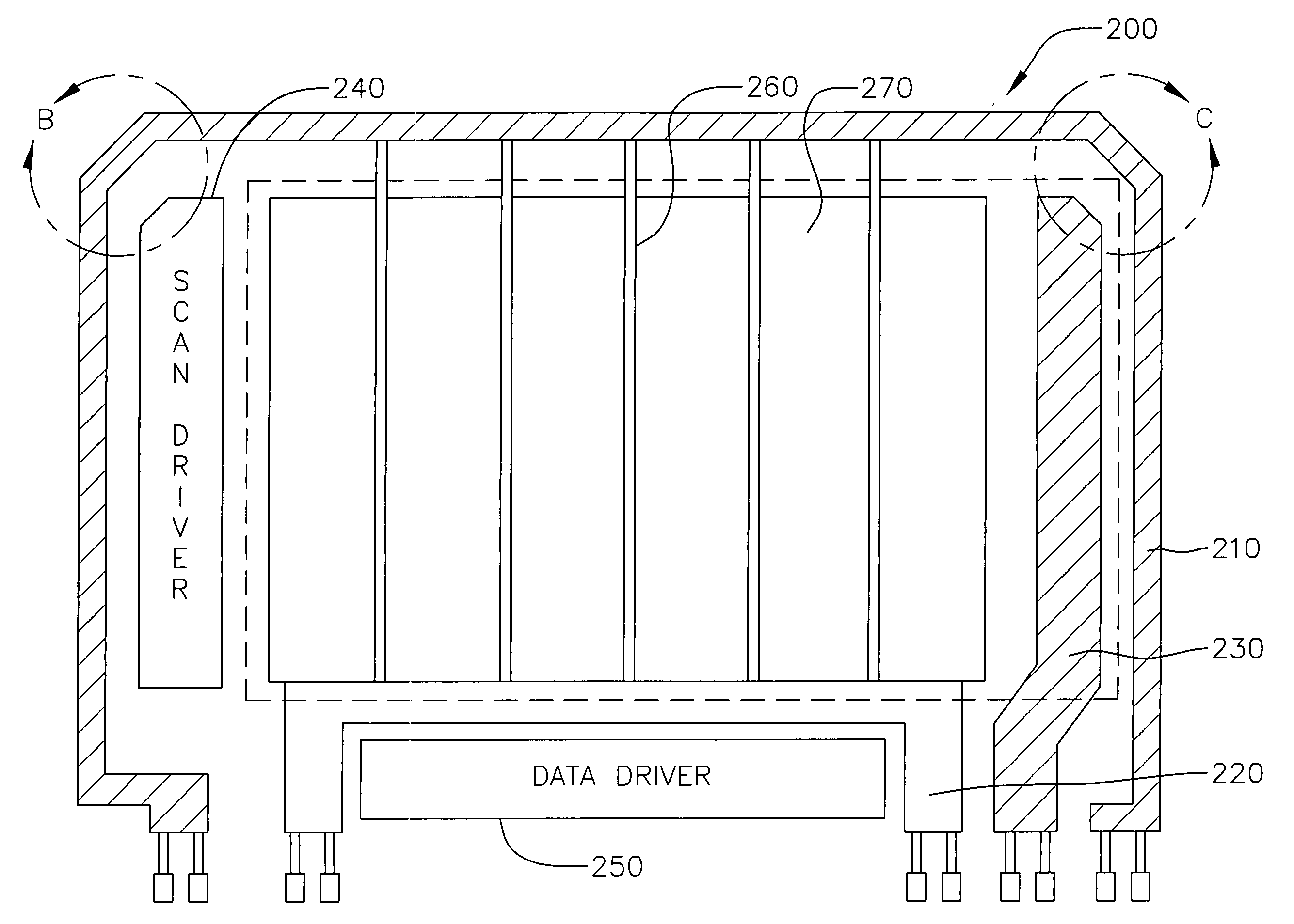
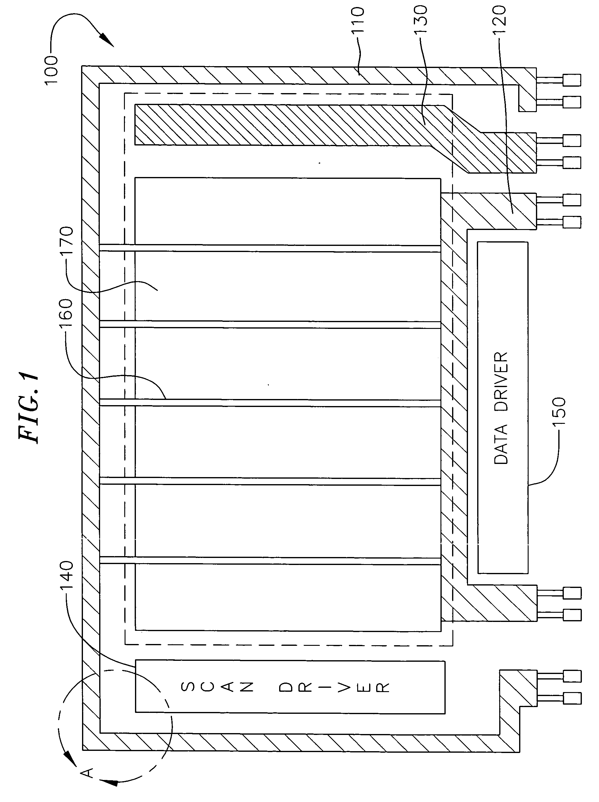
[0029]FIG. 3 is a plan view showing one exemplary embodiment of the present invention.

[0030] An organic electroluminescent display device 200 includes an upper power supply voltage line 210, a lower power supply voltage line 220, a cathode voltage line 230, a scan driver 240, a data driver 250, an active power supply voltage line 260 and a pixel region 270 having a plurality of unit pixels for emitting light of certain colors, formed on a substrate.

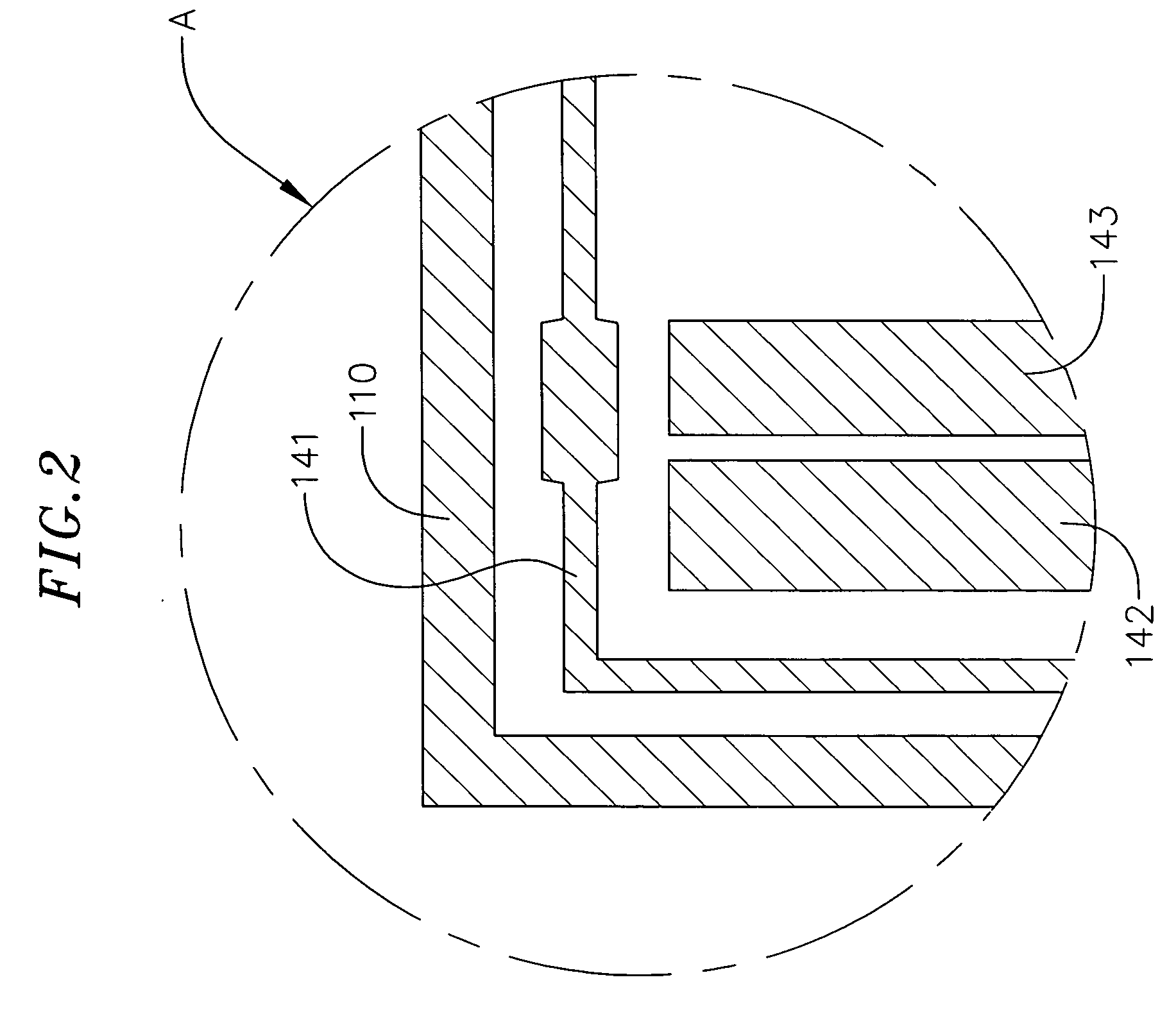
[0031] In FIG. 3, edge parts of the upper power supply voltage line 210 in both parts B, C are formed in an obtuse angle having more than 90 degrees. Additionally, edge parts on wirings adjacent to the edge parts of the upper power supply voltage line 210 should also be formed in an obtuse angle as shown in F...


PUM


Abstract

A display device in which charge damage occurring at wiring near the periphery is prevented or reduced, and wiring is facilitated during manufacturing by controlling an angle of an edge part of the wiring near the periphery. A display device includes a substrate, a pixel region including a plurality of unit pixels formed on the substrate. A power supply voltage line supplies a power supply voltage to the pixel region, and a cathode voltage line supplies a cathode voltage to the pixel region. The power supply voltage line includes an edge part formed in an obtuse angle. The edge part of wiring adjacent to the power supply voltage line may also be formed in an obtuse angle. Further, a cathode voltage line and a scan driver each may include an edge part formed in an obtuse angle. The display device may be an organic electroluminescent display device.

Description

CROSS REFERENCE TO RELATED APPLICATIONS [0001] This application claims priority to and the benefit of Korean Patent Application No. 2003-71594, filed on Oct. 14, 2003, the entire disclosure of which is incorporated herein by reference in its entirety. BACKGROUND OF THE INVENTION [0002] 1. Field of the Invention [0003] The present invention relates to an organic electroluminescent display device, and more particularly, to an organic electroluminescent display device in which charge damage occurring at wiring near the periphery is prevented or reduced, and wiring is facilitated during manufacturing by controlling an angle of an edge part of the wiring near the periphery. [0004] 2. Description of Related Art [0005] Display devices using light emitting elements including organic electroluminescent (EL) device have actively been developed lately. The organic EL device is suitable for a display device having a thin profile and enhanced viewing angles since backlight required in liquid cry...

Claims


Application Information

Patent Timeline
Patent Type & Authority Applications(United States)
IPC IPC(8): G09G3/30G09G5/00H05B33/26H01L27/32H05B33/02H05B33/12
CPCH01L27/3276H10K59/131H05B33/26
Inventor SUH, MI-SOOK
Owner SAMSUNG DISPLAY CO LTD
Why Eureka
Try Eureka