Apparatus and method for mounting electronic components

a technology for electronic components and mounting methods, applied in non-electric welding apparatuses, final product manufacturing,auxillary welding devices, etc., can solve the problems of high-end electronic components not being able to mount high-end electronic components, and high precision for bonding positions

Inactive Publication Date: 2005-05-12
PANASONIC CORP
View PDF24 Cites 76 Cited by
  • Summary
  • Abstract
  • Description
  • Claims
  • Application Information

AI Technical Summary

Benefits of technology

[0091] According to a twenty-sixth aspect of the present invention, there is provided the apparatus for mounting an electronic component according to the twenty-fourth aspect, wherein the detection of the contact load is fulfilled by the control part by detecting that a load generated as a result of moving down the component holding member in very small steps by the up

Problems solved by technology

Therefore, the above-described electronic component mounting performed by the local reflow mounting method, in which suction and holding of an electronic component by the tool is released during a solder's m

Method used


Image

  • Apparatus and method for mounting electronic components
  • Apparatus and method for mounting electronic components
  • Apparatus and method for mounting electronic components

Examples


first embodiment

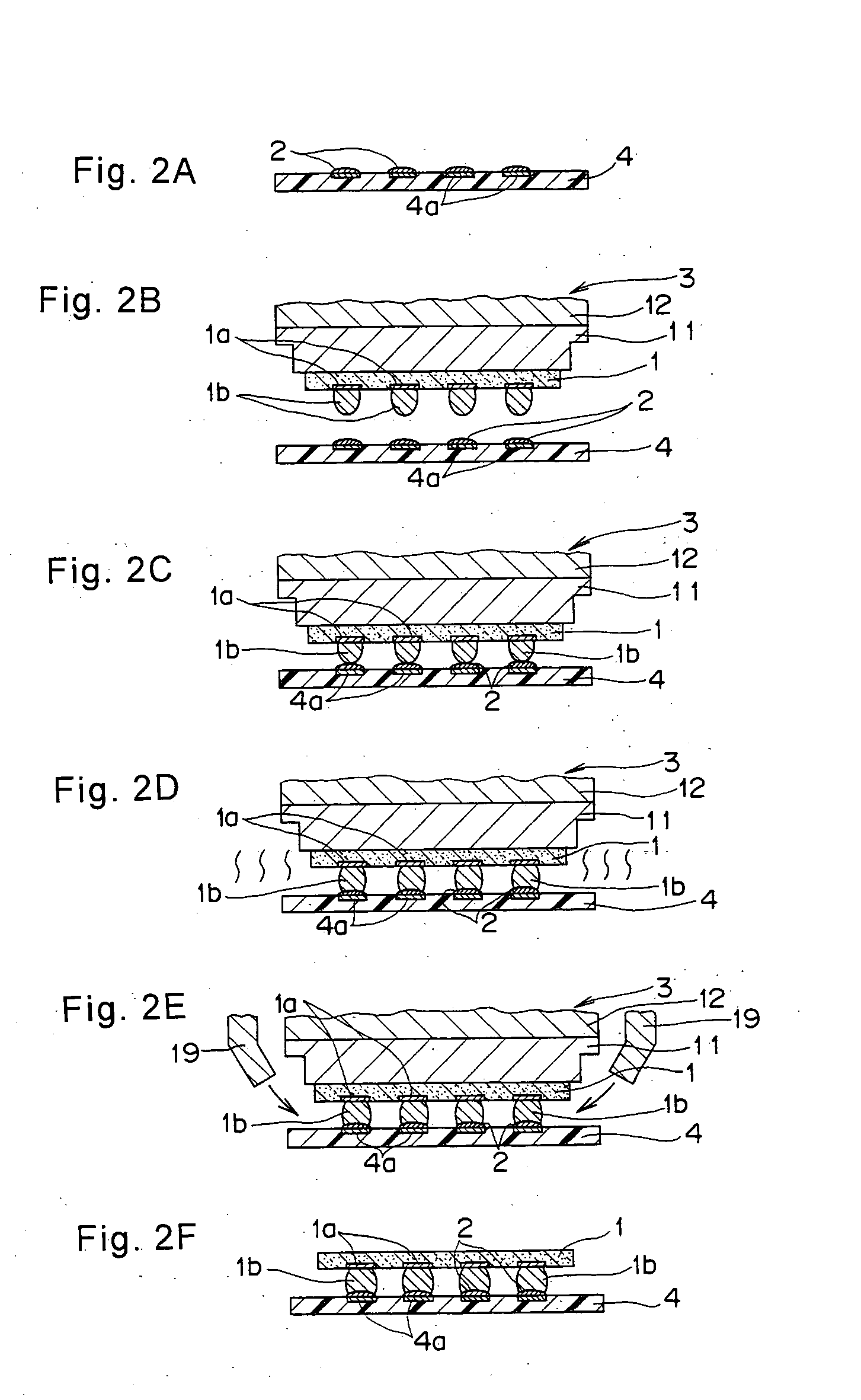
[0147] An electronic component mounting method and apparatus according to the present invention relate to an electronic component mounting method and apparatus including steps of placing a plurality of electrodes of an electronic component and a plurality of electrodes of a circuit board into a state of contact with bonding members interposed therebetween, and causing the bonding members to be individually melted and solidified so that the electronic component is bonded to the circuit board via the bonding members therebetween. An electronic component mounting method and apparatus according to the first embodiment of the invention is described in detail with reference to the accompanying drawings.

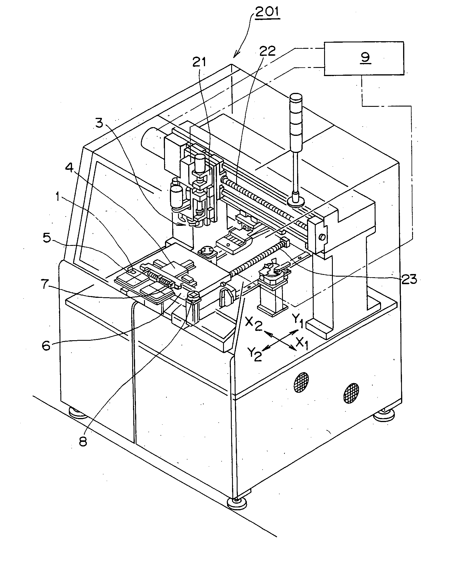
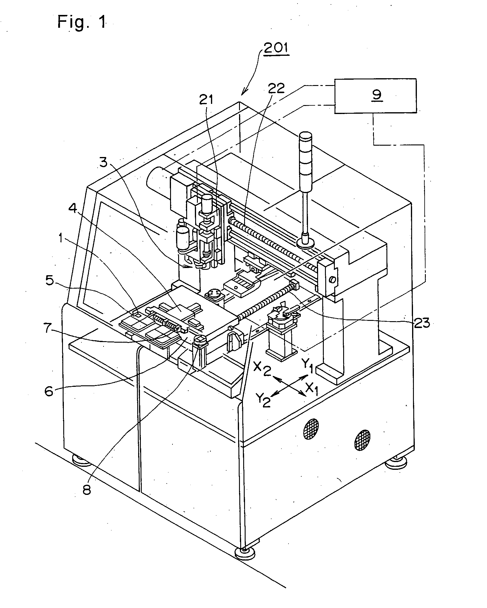
[0148] As shown in FIG. 1, referring to an electronic component mounting apparatus 201, a head tool 3, which is an example of a component holding member for performing electronic component mounting, is fixed to a nut portion of an X-direction moving mechanism 22. The X-direction moving mec...

second embodiment

[0250] It is noted that the present invention is not limited to the above-described embodiment and may be embodied in other various modes. For example, an electronic component mounting method according to a second embodiment of the invention is an electronic component mounting method for mixedly mounting a plurality of types of electronic components onto a circuit board during different methods.

[0251] A first electronic component, which is one type of an electronic component from among the plurality of types of electronic components, is a general-purpose electronic component which is unlikely to incur defective bonding of the electronic component onto a circuit board due to a bonding position shift by virtue of its large bump pitch at which solder bumps are formed at electrodes of the electronic component, respectively, in the conventional collective reflow mounting method even if the bonding position shift of the electronic component with respect to the circuit board has occurred ...

third embodiment

[0269] Further, the mounting apparatus to be used for the electronic component mounting method according to a third embodiment of the invention is an electronic component mounting apparatus in which the head tool further includes a pressing mechanism for pressing an electronic component against a circuit board, wherein the electronic component mounting apparatus employs a head tool that has two large-and-small pneumatic cylinders as an example of the pressing mechanism and that is usable also for local reflow mounting apparatuses, and wherein electronic component mounting can be performed by the local reflow mounting method according to the first embodiment with the electronic component mounting apparatus having this head tool, and moreover the electronic component mounting apparatus is adaptable to local reflow mounting methods.

[0270] Structure of this head tool is explained in detail. Referring to FIG. 14, a head tool 50 comprises a head-tool tip portion 50a for performing suctio...


PUM

PropertyMeasurementUnit
Timeaaaaaaaaaa
Diameteraaaaaaaaaa
Heightaaaaaaaaaa

Abstract

After detection of contact between respective solder bumps of an electronic component, sucked and held by a suction nozzle of a head tool, and respective solder portions of a circuit board, the solder bumps and the solder portions are melted by heating. Releasing of the electronic component from suction and holding by the suction nozzle of the head tool is performed, not at a time during solder melting, but at a time after the solder is melted, cooled and solidified. Thus, an electronic component mounting method and apparatus capable of mounting high-end electronic components having narrow-pitched bumps are provided.

Description

BACKGROUND OF THE INVENTION [0001] The present invention relates to a method and apparatus for mounting electronic components onto a circuit board. More particularly, the invention relates to an electronic component mounting method and apparatus that makes it possible to mount such electronic components as IC chips having narrow pitched bumps onto a circuit board by performing a flip chip bonding method. [0002] As electronic component mounting methods of this type, there have conventionally been known various methods. As an example of a conventional electronic component mounting method corresponding to the flip chip bonding method, is a method including steps of temporarily bonding a plurality of electronic components onto a circuit board and thereafter subjecting the electronic components collectively to reflow soldering, thus achieving electronic component mounting, (hereinafter, described as a collective reflow mounting method) as shown FIGS. 22A-22D. [0003] As shown in FIG. 22A,...

Claims


Application Information

Patent Timeline
IPC IPC(8): B23K1/00H01L21/56H01L21/60H05K3/34
CPCB23K1/0016H01L2224/73204H01L21/563H01L24/75H01L24/81H01L2224/13144H01L2224/16H01L2224/75H01L2224/751H01L2224/7515H01L2224/75301H01L2224/755H01L2224/758H01L2224/7598H01L2224/81801H01L2224/83192H01L2924/01052H01L2924/01073H01L2924/01078H01L2924/01079H01L2924/01082H01L2924/01322H01L2924/09701H01L2924/14H05K3/3436H05K3/3494H05K2201/10151H05K2203/0195H05K2203/082B23K2201/40H01L2924/014H01L2924/01005H01L2924/01006H01L2924/01023H01L2924/01033H01L2924/01043H01L2924/01065H01L2924/01075H01L2924/00014B23K2101/40H01L2224/05571H01L2224/05573H01L2224/75502H01L2224/92125Y02P70/50H01L2224/05599
Inventor ONOBORI, SHUNJIHIRATA, SHUICHIYAMANO, MASAKAZUYAMAMOTO, KAZUYASHIDA, SATOSHIMAE, TAKAHARUAKITA, MAKOTOMINAMITANI, SHOZO
Owner PANASONIC CORP
Why Eureka
Try Eureka