Electro-absorptive optical modulator module having monolithic integrated photo detector

Active Publication Date: 2005-06-16
SAMSUNG ELECTRONICS CO LTD
View PDF7 Cites 11 Cited by
  • Summary
  • Abstract
  • Description
  • Claims
  • Application Information

AI Technical Summary

Benefits of technology

[0022] The present invention has been made to solve at least some of the above-mentioned problems. It is an aspect of the present invention to provide an electro-absorptive optical mo

Problems solved by technology

However, one of the problems with a conventional light source is that there must be a separate modulation means for converting an electrical signal into a modulated optical signal.
In addition, there are problems associated with using the conventional light source, such as an increase in the number of manufacturing processes required, a larger percentage of defects, both of which increase the unit costs of production.
Therefore, as it is n

Method used


Image

  • Electro-absorptive optical modulator module having monolithic integrated photo detector
  • Electro-absorptive optical modulator module having monolithic integrated photo detector
  • Electro-absorptive optical modulator module having monolithic integrated photo detector

Examples


Example

[0033] Hereinafter, preferred aspects of an electro-absorptive optical modulator module having a monolithic integrated photo detector according to the present invention will be described with reference to the accompanying drawings. For the purposes of clarity and simplicity, a detailed description of known functions and configurations incorporated herein will be omitted as it may obscure the subject matter of the present invention.

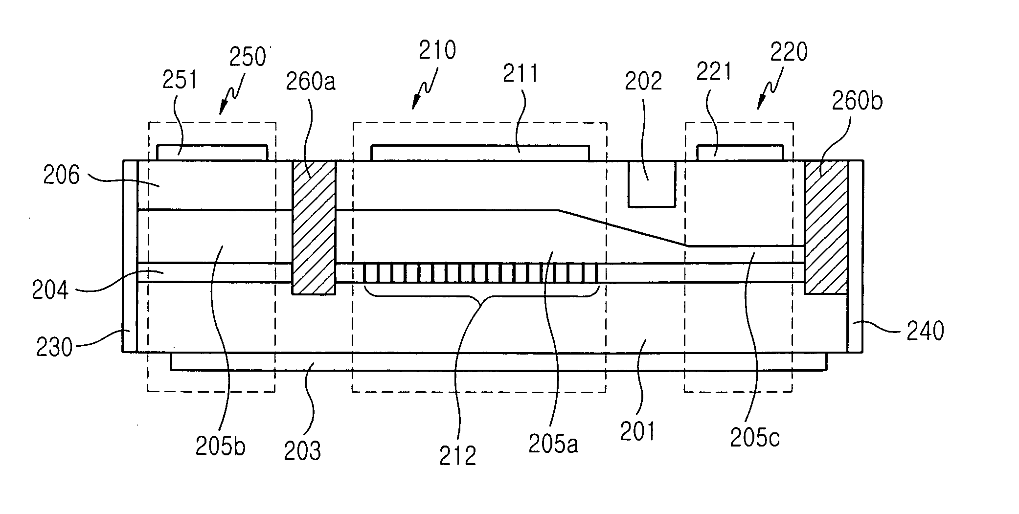
[0034]FIG. 2 illustrates a construction of a monolithic integrated electro-absorptive optical modulator module according to a first aspect of the present invention. Referring to FIG. 2, the monolithic integrated electro-absorptive optical modulator module includes a distributed feedback laser 210 having a grating for oscillating light, an electro-absorptive modulator 220, an optical detector 250 for detecting a second light, a first inner window 260a formed between the distributed feedback laser 210 and the optical detector 250, a second inner window 260b...


PUM


Abstract

An electro-absorptive optical modulator module monolithic-integrated on a semiconductor substrate, which includes a distributed feedback laser having a grating for oscillating light and to output the oscillated light through a first end and a second end of the module. An electro-absorptive modulator modulates a first light output through the first end of the distributed feedback laser, and an optical detector provides detection of a second light output through the second end of the module. The optical detector is formed opposite to the second end of the distributed feedback laser on the semiconductor substrate. A first inner window permits attenuation of the intensity of the second light and electrically insulates the distributed feedback laser and the optical detector from each other, with the first inner window being arranged between the distributed feedback laser and the optical detector.

Description

CLAIM OF PRIORITY [0001] This application claims priority from an application entitled “Electro-absorptive optical modulator module having monolithic integrated photo detector,” filed in the Korean Intellectual Property Office on Dec. 16, 2003 and assigned Serial No. 2003-91891, the contents of which are hereby incorporated by reference. BACKGROUND OF THE INVENTION [0002] 1. Field of the Invention [0003] The present invention relates to a light source for optical communication. More particularly, the present invention relates to an optical modulator module including a distributed feedback laser. [0004] 2. Description of the Related Art [0005] Optical communication has several advantages over standard electrical communication in that optical communication can simultaneously transmit more signals to a long-distance destination, as compared with normal transmission of electric signals. As a light source of the above-mentioned optical communication, a laser capable of outputting coheren...

Claims


Application Information

Patent Timeline
IPC IPC(8): G02B6/12G02F1/03G02F1/07G02F1/017H01S3/00H01S5/12H01S5/026
CPCH01S5/0264H01S5/0265H01S5/1203H01S5/1064H01S5/12H01S5/106G02B6/12
Inventor KIM, INKIM, YOUNG-HYUNKANG, BYUNG-KWON
Owner SAMSUNG ELECTRONICS CO LTD
Why Eureka
Try Eureka