

Selective nitridation of gate oxides
a gate oxide and selective nitridation technology, applied in the direction of semiconductor devices, electrical equipment, transistors, etc., can solve the problems of increasing leakage current through the dielectric, and affecting the efficiency of the dielectri
- Summary
- Abstract
- Description
- Claims
- Application Information
AI Technical Summary
Benefits of technology
Problems solved by technology
Method used
Image

Examples
Embodiment Construction
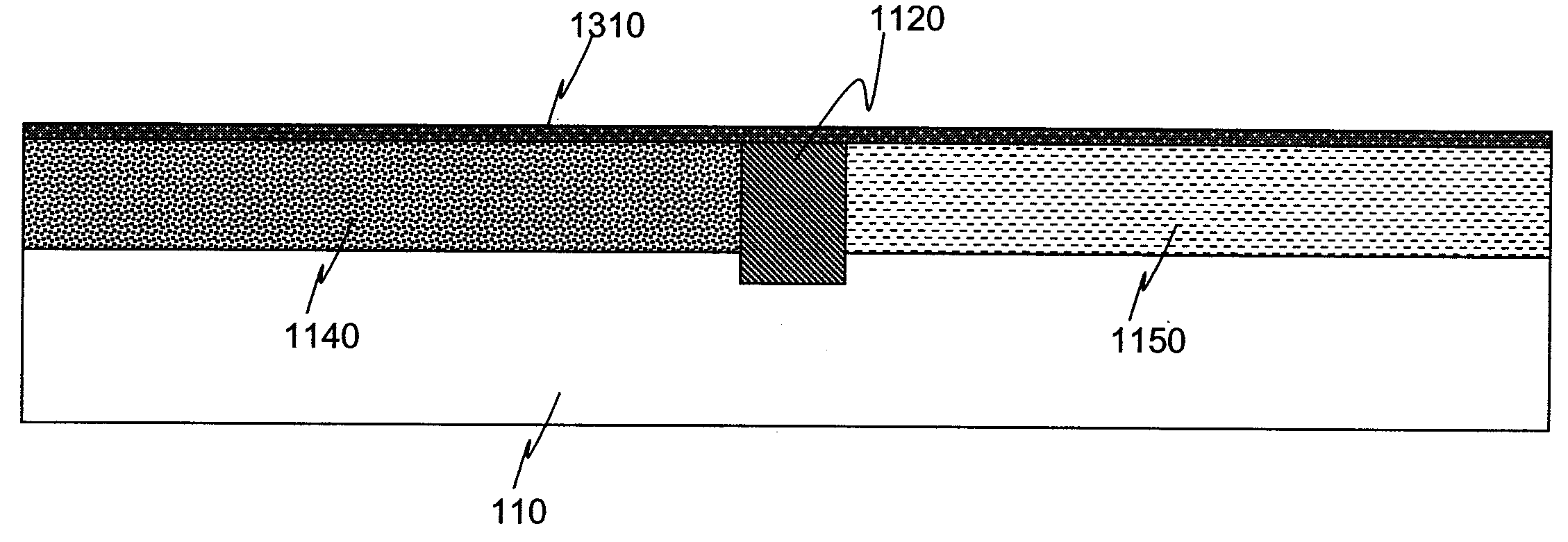
[0025] The invention enables independently introducing nitrogen into (i.e., nitridation of) nFET and pFET gate dielectrics. The amount of nitrogen introduced is sufficient to reduce or prevent gate leakage and dopant penetration, without appreciably degrading device performance. An exemplary implementation introduces a lower concentration of nitrogen into pFET gate dielectrics than into nFET gate dielectrics, and a low concentration, no nitrogen, or a high concentration into areas having thick gate dielectric that are not susceptible to appreciable dopant diffusion and current leakage.
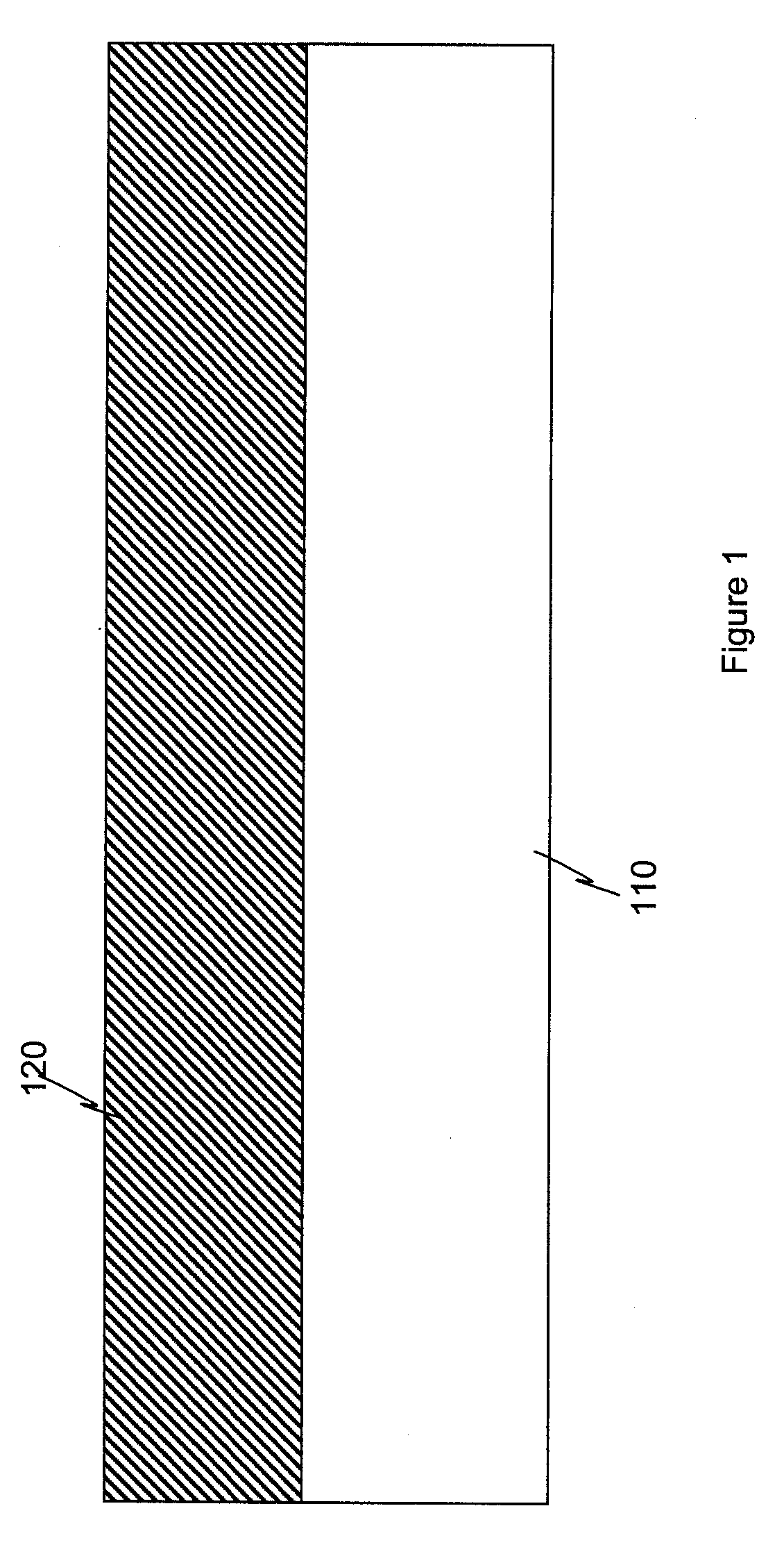
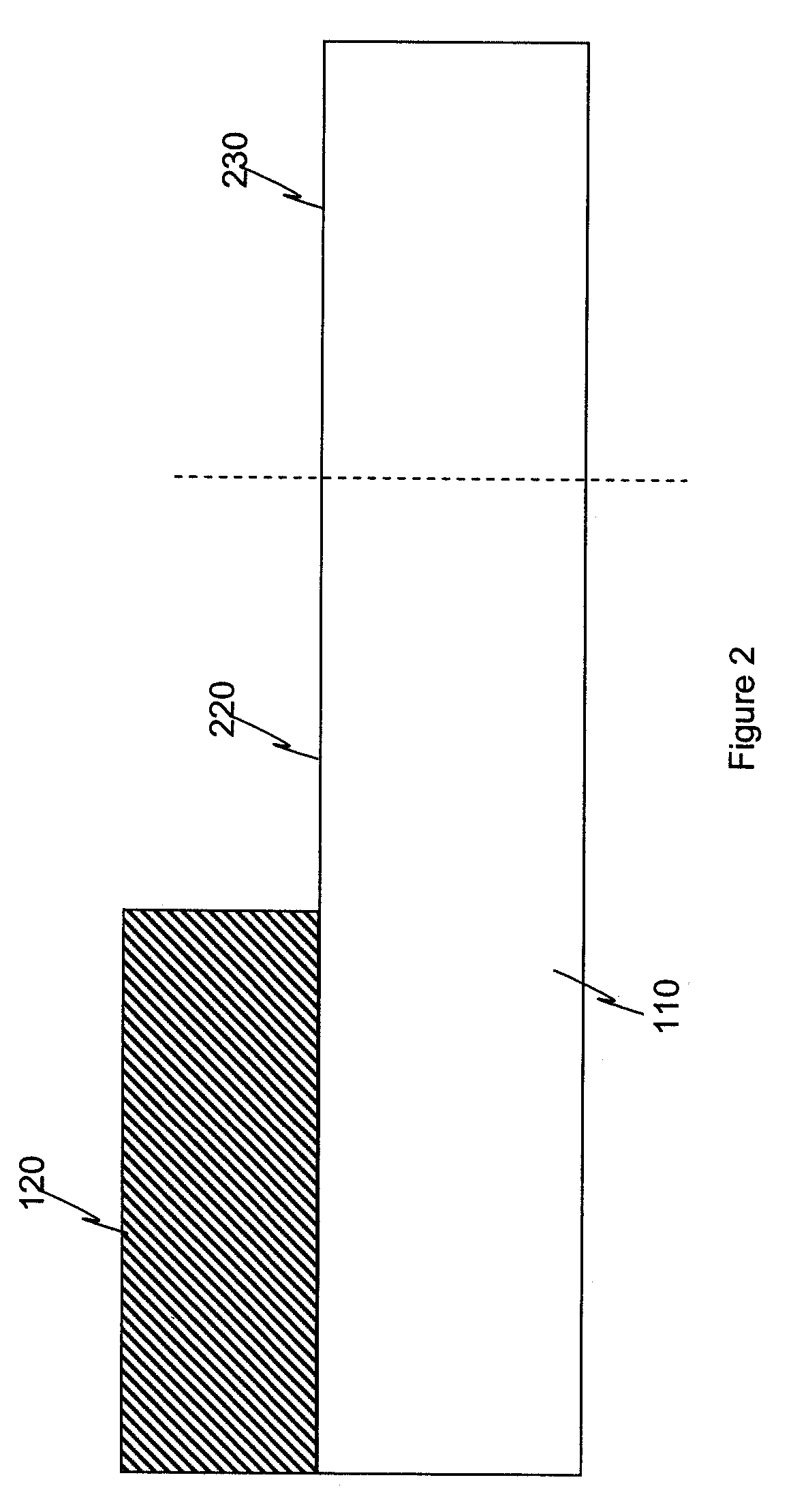
[0026] In one implementation, a semiconductor device including a substrate 110 and gate dielectric layer 120 is formed in a conventional manner, as shown in FIG. 1. A process according to the principles of the invention modifies portions of the device before formation of the gate electrode which overlies the gate dielectric, and before formation of spacers which surround the gate electrode.
[0027] The...
PUM
 Abstract
Description
Claims
Application Information